What are electronics made of?
Overview
In this tutorial, we're going to be talking about the different elements that make up a Printed Circuit Board (PCB). For each element, we'll show different ways that the element can be represented in tscircuit.
What is copper? Why are PCBs green?
Copper is a conductive material that's used on a PCB to make an electrical connection between chips. A PCB is mostly made up of fiberglass with a small layer of precisely etched copper. The fiberglass is non-conductive and often coated with non-conductive green "soldermask" to cover parts of the copper that aren't meant to be connected to chips.
A PCB can be thought of as a bunch of "printed" copper separated by fiberglass sections that "insulate" or don't conduct electricity. We "glue" (solder) chips to the copper "pads" to add them to the circuit.
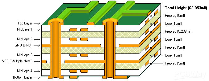
What are PCB layers?
When you print on a piece of paper, you can print "single-sided" or "double-sided", PCBs can also be printed singled-sided or double-sided! The "front" of the PCB is called the "top" layer, and the "back" of the PCB is called the "bottom" layer.
We can "print" copper to each of these layers to draw lots of wires and connect lots of chips. Sometimes a wire needs to "go over"/"go under" another wire because the wires aren't allowed to cross. When this happens, we can use the "back" or "bottom layer" of the PCB to draw the wire so that the wires don't accidentally touch.
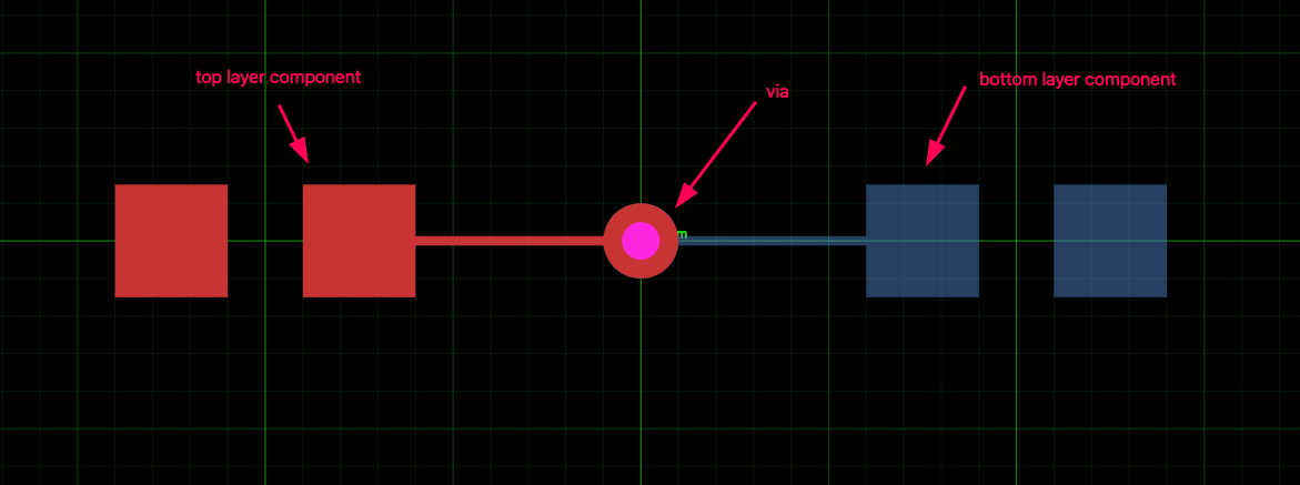
Vias
Vias are holes that connect different layers of PCB. Let's say you have a chip on the top layer of a PCB and the back layer of a PCB. How can you connect them? The copper on the top needs some way to "pass through" to the bottom layer.
This is where vias come in. A via is a hole that is "filled with copper" so that the top layer can pass to the bottom.
Plated Holes
A plated hole is similar to a via but it's hollow so that you can push metal pins through it. This is important for chips that have big pins that need to fit into holes. Chips with big pins that must go through holes are called "through-hole" chips, and chips with small pins are called "surface-mount" chips.
Unplated Holes "Regular Holes"
Unplated holes or "regular holes" are just holes in the printed circuit board without any copper around them. They don't electrically connect anything, but can be very helpful for mounting the printed circuit board.
Traces
Traces are the wires that connect the components on a PCB. They are made of copper and mostly covered by green soldermask so that they don't accidentally conduct to each other if something conductive like a wire or piece of metal falls across them.
We represent traces in PCB viewers with different colors depending on what layer they fall on. In tscircuit, traces are always autorouted, so you don't need to tell it which path to take- it'll automatically find one that makes sure it doesn't cross any other traces.
Traces allow chips to "talk" to each other and for power to be shared across all chips.
What are inner layers?
Inner layers are layers of PCB that aren't visible, they're sandwiched on the inside. Sometimes this is useful when you have a lot of wires to connect and it's almost impossible to stop them from crossing each other.