This file is a merged representation of a subset of the codebase, containing specifically included files, combined into a single document by Repomix.
This section contains a summary of this file.
This file contains a packed representation of the entire repository's contents.
It is designed to be easily consumable by AI systems for analysis, code review,
or other automated processes.
The content is organized as follows:
1. This summary section
2. Repository information
3. Directory structure
4. Repository files (if enabled)
5. Multiple file entries, each consisting of:
- File path as an attribute
- Full contents of the file
- This file should be treated as read-only. Any changes should be made to the
original repository files, not this packed version.
- When processing this file, use the file path to distinguish
between different files in the repository.
- Be aware that this file may contain sensitive information. Handle it with
the same level of security as you would the original repository.
- Some files may have been excluded based on .gitignore rules and Repomix's configuration
- Binary files are not included in this packed representation. Please refer to the Repository Structure section for a complete list of file paths, including binary files
- Only files matching these patterns are included: **/*.md, **/*.mdx
- Files matching patterns in .gitignore are excluded
- Files matching default ignore patterns are excluded
- Files are sorted by Git change count (files with more changes are at the bottom)
docs/
advanced/
ai-context.mdx
create-or-use-custom-autorouter.mdx
local-package-development.mdx
math-utils.mdx
simple-route-json.mdx
units.md
building-electronics/
designing-electronics-from-scratch.md
ordering-prototypes.mdx
what-are-electronics-made-of.mdx
command-line/
tsci-add.mdx
tsci-auth-print-token.md
tsci-build.md
tsci-check.md
tsci-clone.md
tsci-config.md
tsci-convert.md
tsci-dev.md
tsci-doctor.md
tsci-export.md
tsci-import.md
tsci-init.md
tsci-install.md
tsci-login.md
tsci-push.md
tsci-remove.md
tsci-search.md
tsci-simulate.md
tsci-snapshot.md
tsci-transpile.md
contributing/
bounties-and-sponsorship.md
contributing-autorouting-dataset.md
getting-started-as-a-contributor.md
making-lab-boards.mdx
overview-of-projects.md
package-dependencies-and-auto-updates.mdx
report-autorouter-bugs.md
the-contributor-handbook.md
elements/
ammeter.mdx
analogsimulation.mdx
autoroutingphase.mdx
battery.mdx
board.mdx
breakout.mdx
breakoutpoint.mdx
cadassembly.mdx
cadmodel.mdx
capacitor.mdx
chip.mdx
connector.mdx
copperpour.mdx
coppertext.mdx
courtyardcircle.mdx
courtyardoutline.mdx
courtyardrect.mdx
crystal.mdx
cutout.mdx
diode.mdx
drccheck.mdx
fiducial.mdx
footprint.mdx
fuse.mdx
group.mdx
hole.mdx
inductor.mdx
jumper.mdx
keepout.mdx
led.mdx
mosfet.mdx
net.mdx
netlabel.mdx
opamp.mdx
pcbnotedimension.mdx
pcbnoteline.mdx
pcbnotepath.mdx
pcbnoterect.mdx
pcbnotetext.mdx
pinheader.mdx
port.mdx
potentiometer.mdx
pushbutton.mdx
resistor.mdx
resonator.mdx
schematicarc.mdx
schematiccircle.mdx
schematicline.mdx
schematicpath.mdx
schematicrect.mdx
schematicsection.mdx
schematicsheet.mdx
schematictable.mdx
schematictext.mdx
solderjumper.mdx
spicemodel.mdx
subcircuit.mdx
switch.mdx
symbol.mdx
testpoint.mdx
trace.mdx
transistor.mdx
via.mdx
voltageprobe.mdx
voltagesource.mdx
footprints/
constraint.mdx
fabricationnoterect.mdx
fabricationnotetext.mdx
footprint-elements-vs-footprint-strings.mdx
footprinter-strings.mdx
jlcpcb-footprints.mdx
kicad-footprints.mdx
platedhole.mdx
silkscreencircle.mdx
silkscreengraphic.mdx
silkscreenline.mdx
silkscreenpath.mdx
silkscreenrect.mdx
silkscreentext.mdx
smtpad.mdx
guides/
circuit-generation/
generating-circuit-boards-with-ai.mdx
importing-modules-and-chips/
importing-from-circuit-json.mdx
importing-from-jlcpcb.mdx
importing-from-kicad.md
installing-kicad-libraries-from-github.md
using-tscircuit-ti-library.mdx
kicad/
exporting-kicad-library.md
kicad-metadata.mdx
using-tscircuit-kicad-pcm-urls.md
running-tscircuit/
scripting/
measuring-circuit-size.mdx
building-static-sites-with-tsci.mdx
connecting-to-github.mdx
displaying-circuit-json-on-a-webpage.mdx
platform-configuration.md
programmatically-building-circuits.md
running-tscircuit-inside-an-iframe.mdx
running-tscircuit-standalone.mdx
using-tscircuit-without-react.mdx
spice-simulation/
Diodes/
full-wave-rectifier.mdx
half-wave-rectifier.mdx
Passive Filters/
high-pass-filter.mdx
low-pass-filter.mdx
Power Converters/
boost-converter.mdx
Transistors/
transistor-switch-example.mdx
introduction.mdx
tscircuit-essentials/
automatic-pcb-layout.mdx
automatic-schematic-layout.mdx
configuring-chips.mdx
draw-a-wifi-antenna.mdx
essential-elements.mdx
layout-properties.mdx
manual-edits.mdx
panelization.mdx
pcb-sx.mdx
pinout-svg.mdx
port-and-net-selectors.md
relative-positioning.mdx
restyling-schematics-with-css-classes.mdx
single-layer-jumper-autorouting.mdx
tscircuit-config.mdx
using-expressions.mdx
using-groups-for-pcb-layout.mdx
using-sel-references.mdx
using-viagrid-prefabricated-vias-with-autorouter.mdx
typescript-guide/
using-react-context-to-avoid-prop-drilling.mdx
using-typescript-path-aliases.mdx
distributing-tscircuit-libraries.md
understanding-fabrication-files.md
intro/
installation.md
quickstart-ChatGPT.mdx
quickstart-cli.md
quickstart-web.md
what-is-tscircuit.mdx
tutorials/
pi-hats/
simple-buzzer-hat.mdx
build-a-custom-keyboard-with-tscircuit.mdx
building-a-simple-usb-flashlight.mdx
building-led-matrix.mdx
web-apis/
autorouting-api.mdx
compile-api.md
datasheet-api.md
datasheet-sdk.md
finding-package-releases.md
image-generation-api.mdx
jlcsearch-api.md
ordering-api.mdx
package-builds-create-api.md
package-builds-get-api.md
package-files-download-api.md
package-files-list-api.md
package-releases-get-api.md
package-releases-list-api.md
the-registry-api.md
static/
templates/
AGENTS.md
AGENTS.md
CLAUDE.md
README.md
This section contains the contents of the repository's files.
---
title: Use tscircuit with AI
description: Install the tscircuit skill so your AI assistant can design boards with tscircuit
---
import YouTubeEmbed from '../../src/components/YouTubeEmbed';
## Overview
To use tscircuit with an AI assistant, install the `tscircuit` skill:
```bash
npx skills add tscircuit/skill
```
The skill lives in the [tscircuit/skill](https://github.com/tscircuit/skill)
repository.
It contains the syntax, workflows, CLI usage, and project knowledge an AI needs
to build a board from scratch with tscircuit.
After installing it, tell the AI what you want to build, any physical
constraints, and which parts or interfaces you need. The skill gives the AI the
context it needs to search for components, write tscircuit code, and iterate on
your design.
---
title: Local Package Development
description: Learn how to develop and test local packages with tsci dev using yalc and other linking tools
---
## Overview
When developing tscircuit projects, you may want to test changes to local packages without publishing them to npm. The `tsci dev` command automatically detects and uploads local packages, making local development seamless.
Currently supported methods:
- **yalc** - Recommended for most use cases
- **bun link** - Native Bun linking for Bun users
## What is Yalc?
[Yalc](https://github.com/wclr/yalc) is a tool for managing local package dependencies. It's a better alternative to `npm link` that creates a local package store and symlinks packages into your project's `node_modules`.
## Installation
First, install yalc globally:
```bash
npm install -g yalc
# or
bun install -g yalc
```
## Basic Workflow
### 1. Build and Publish Your Local Package
In the package you're developing `@/` (e.g., `@tscircuit/pico`):
```bash
cd path/to/your/local/package
# Build the package first
bun run build
# or npm run build
# Then publish to yalc
yalc publish
```
This builds the package and publishes the distribution files to your local yalc store.
**Note**: You must build the package before publishing with yalc, as it publishes the compiled output (typically in `dist/` or `lib/`), not the source files.
### 2. Link the Package to Your Project
In your tscircuit project:
```bash
cd path/to/your/tscircuit-project
yalc add @tscircuit/pico
```
This will:
- Add the package to your `node_modules`
- Update your `package.json` with a `file:.yalc/@tscircuit/pico` reference
- Create a `.yalc` directory with the package contents
### 3. Start Development
Run the dev server as usual:
```bash
tsci dev index.circuit.tsx
```
The dev server will automatically detect that `@tscircuit/pico` is a local package (via the `file:.yalc/` reference) and upload it along with your component files.
### 4. Update Your Local Package
When you make changes to your local package:
```bash
# In the local package directory
bun run build # Rebuild with your changes
yalc push # Push updates to all linked projects
```
This will rebuild and update all linked projects. You may need to restart `tsci dev` to pick up the changes.
## How It Works
The `tsci dev` command automatically uploads packages from `node_modules` **only if** they meet these criteria:
1. The package is referenced in `package.json` with a `file:.yalc/` path
2. The package exists in your `node_modules` directory
Regular npm packages (like `react`, `lodash`, etc.) are **not** uploaded to keep bundle sizes small and development fast.
## Example
Here's a complete example of developing a custom component library:
**Your local library** (`my-components`):
```tsx
// my-components/src/index.ts
export const MyCustomChip = (props: any) => {
return
}
```
**Publish it locally**:
```bash
bun run build
yalc publish
```
**Use it in your project**:
```bash
cd my-tscircuit-project
yalc add my-components
```
**Your component**:
```tsx
// circuit.tsx
import { MyCustomChip } from "my-components"
export default () => (
)
```
**Start dev server**:
```bash
tsci dev circuit.tsx
```
Now both your component and the `my-components` package code will be uploaded to the dev server!
## Removing Yalc Packages
To remove a yalc package and restore the npm version:
```bash
yalc remove @tscircuit/pico
npm install @tscircuit/pico
```
Or remove all yalc packages:
```bash
yalc remove --all
```
## Tips
- Use `yalc push` instead of `yalc publish` when updating packages - it's faster and automatically updates linked projects
- The `.yalc` directory and `yalc.lock` file should be added to `.gitignore`
- Remember to test with the published npm version before releasing to ensure compatibility
## Using Bun Link
If you're using Bun as your package manager, you can use the native `bun link` command instead of yalc. This provides a simpler workflow for Bun users.
### Basic Workflow with Bun Link
#### 1. Link Your Local Package
In the package you're developing (e.g., `@tscircuit/pico`):
```bash
cd path/to/your/local/package
# Build the package first
bun run build
# Register it for linking
bun link
```
This registers the package globally, making it available for linking in other projects.
#### 2. Link the Package to Your Project
In your tscircuit project:
```bash
cd path/to/your/tscircuit-project
bun link @tscircuit/pico
```
This creates a symlink in your project's `node_modules` pointing to your local package.
#### 3. Start Development
Run the dev server as usual:
```bash
tsci dev index.circuit.tsx
```
The dev server will automatically detect that `@tscircuit/pico` is a local package (via the symlink) and upload it along with your component files.
#### 4. Update Your Local Package
When you make changes to your local package:
```bash
# In the local package directory
bun run build # Rebuild with your changes
```
Since `bun link` uses symlinks, the changes will be immediately available. You may need to restart `tsci dev` to pick up the changes.
### Unlinking Bun Packages
To remove a linked package:
```bash
# In your project
bun unlink @tscircuit/pico
```
To remove the global link registration:
```bash
# In the package directory
bun unlink
```
---
title: Math Utils
description: >-
The `@tscircuit/math-utils` package provides a set of utilities that are
commonly used in circuit design. The `@tscircuit/math-utils` package is
generally available in any platform that uses `tscircuit`.
---
## Overview
The `@tscircuit/math-utils` package provides a set of utilities that are
commonly used in circuit design. The `@tscircuit/math-utils` package is
generally available in any platform that uses `tscircuit`.
The source code for the `@tscircuit/math-utils` package [is available here](https://github.com/tscircuit/math-utils)
## `grid`
A utility function that generates a grid of cells with configurable dimensions, spacing, and positioning. Each cell contains its index, position (row/column), and coordinate points (center, top-left, bottom-right).
(
{gridCells.map((cell) => (
))}
)
`}
/>
## Grid Options
| Option | Description | Default |
| ------ | ----------- | ------- |
| `rows` | Number of rows in the generated grid. | Required |
| `cols` | Number of columns in the generated grid. | Required |
| `width` | Total width of the grid. When omitted, uses `cols * xSpacing`. | `cols * xSpacing` |
| `height` | Total height of the grid. When omitted, uses `rows * ySpacing`. | `rows * ySpacing` |
| `xSpacing` | Horizontal spacing between cells when `width` is not provided. | `1` |
| `ySpacing` | Vertical spacing between cells when `height` is not provided. | `1` |
| `offsetX` | Horizontal offset applied to every cell. | `0` |
| `offsetY` | Vertical offset applied to every cell. | `0` |
| `yDirection` | Sets positive Y direction: `"cartesian"` keeps positive-up, `"up-is-negative"` flips it. | `"cartesian"` |
| `centered` | Centers the grid around the origin when `true`. | `true` |
## Grid Cell Data
Each object returned by `grid` represents a cell with useful positional metadata:
| Property | Description |
| -------- | ----------- |
| `index` | Sequential identifier for the cell. |
| `row` / `col` | Grid coordinates of the cell starting from zero. |
| `center` | `{ x, y }` coordinates of the cell center. |
| `topLeft` | `{ x, y }` coordinates of the cell's top-left corner. |
| `bottomRight` | `{ x, y }` coordinates of the cell's bottom-right corner. |
---
title: Simple Route JSON
description: >-
Simple Route JSON (SRJ) is a lightweight, straightforward format designed to
describe a Printed Circuit Board (PCB) routing problem. It serves as a common
intermediary representation used by `tscircuit` autorouters, simplifying the
complex details often found in full PCB design files.
---
## Overview
Simple Route JSON (SRJ) is a lightweight, straightforward format designed to describe a Printed Circuit Board (PCB) routing problem. It serves as a common intermediary representation used by [`tscircuit` autorouters](https://github.com/tscircuit/unravel-autorouter), simplifying the complex details often found in full PCB design files.
The primary goal of SRJ is to provide only the essential information required for a routing algorithm:
1. Where routing is allowed (layers, board boundaries).
2. Where routing is forbidden (obstacles, keep-out areas).
3. What needs to be connected (nets and their associated pins/pads).
4. Basic routing constraints (minimum trace width).
SRJ can be directly generated from more comprehensive formats like [Circuit JSON](https://circuitjson.com), stripping away details irrelevant to the core routing task (e.g., specific component models, schematic information beyond connectivity). It shares conceptual similarities with the industry-standard [Specctra DSN (Design)](https://github.com/tscircuit/dsn-converter) format, but aims for greater simplicity and modern JSON representation.
:::info
A formal specification with versioning is planned for the future. To stay updated on its release and other tscircuit developments, please subscribe to [the tscircuit newsletter](https://blog.tscircuit.com/).
:::
## Format Structure
A Simple Route JSON file is a single JSON object containing the definition of the board layout, obstacles, and connections needed for routing.
```typescript
export interface SimpleRouteJson {
/** The total number of conductive layers on the PCB. */
layerCount: number;
/** The default or minimum width for traces. Specific trace segments might override this if the format evolves, but currently used as a general guideline. Units are implicit (e.g., mm, inches) and must be consistent throughout the file. */
minTraceWidth: number;
/** An array of obstacles on the board, such as component pads, mounting holes, or keep-out areas. */
obstacles: Obstacle[];
/** An array defining the electrical connections (nets) that need to be routed. */
connections: Array;
/** The bounding box defining the extents of the routing area. */
bounds: { minX: number; maxX: number; minY: number; maxY: number };
/** [Optional] The routing solution provided by an autorouter. This array contains the actual paths of the traces. It is typically absent in the input file given to a router and present in the output file. */
traces?: SimplifiedPcbTrace[];
}
```
## Top-Level Properties
### `layerCount`
* **Type:** `number`
* **Description:** An integer specifying the total number of conductive layers available for routing on the PCB. Layers are typically identified by string names (e.g., `"top"`, `"inner1"`, `"bottom"`) within other parts of the format (like `obstacles` and `connections`). While `layerCount` provides the total number, the specific layer names used must be consistent throughout the file.
### `minTraceWidth`
* **Type:** `number`
* **Description:** Specifies the default or minimum trace width to be used by the autorouter. This acts as a global constraint. Future versions or specific router implementations might allow per-net or per-segment width rules, but this provides a baseline.
* **Units:** Units (e.g., millimeters, inches) are not explicitly defined by the format. It is crucial that the same unit system is used consistently for all dimensional values (`minTraceWidth`, `obstacles`, `bounds`, coordinates) within a single SRJ file. Millimeters (mm) are commonly used.
### `obstacles`
* **Type:** `Array`
* **Description:** An array containing objects that represent areas on the PCB where routing is either restricted or represents a connection point. Obstacles can be physical component pads, mounting holes, board edges defined as keep-outs, or explicit keep-out zones.
```typescript
export type Obstacle = {
/** The shape of the obstacle. Currently, only "rect" is standard. Oval shapes might be included in future revisions. */
type: "rect"; // NOTE: most datasets do not contain ovals
/** An array of layer names (strings) on which this obstacle exists. An obstacle can span multiple layers (e.g., a plated through-hole pad). */
layers: string[];
/** The center coordinates of the obstacle. */
center: { x: number; y: number };
/** The width of the rectangular obstacle. */
width: number;
/** The height of the rectangular obstacle. */
height: number;
/** An array of connection names (strings) that this obstacle is part of. If this obstacle is a pad for a net (e.g., "GND", "VCC"), the net name(s) will be listed here. If the array is empty, the obstacle is typically a keep-out area or an unconnected feature. */
connectedTo: string[];
};
```
* **`type`**: Defines the geometry. Currently `"rect"` is the standard.
* **`layers`**: Specifies which layer(s) the obstacle occupies. Important for multi-layer routing.
* **`center`, `width`, `height`**: Define the geometry and position of the rectangle. Units must be consistent with `minTraceWidth` and `bounds`.
* **`connectedTo`**: This critical field links obstacles (like pads) to the electrical nets defined in the `connections` array. If an obstacle represents a pin for the "VCC" net, `connectedTo` would contain `["VCC"]`.
### `connections`
* **Type:** `Array`
* **Description:** Defines the sets of points that need to be electrically connected. Each object in the array represents a single net (e.g., power, ground, signal).
```typescript
export interface SimpleRouteConnection {
/** The unique name of the connection or net (e.g., "GND", "VCC", "DATA0"). This name is referenced by Obstacle.connectedTo. */
name: string;
/** An array of points that must be connected together to form this net. Each point typically corresponds to the center of an obstacle (pad) belonging to this net. */
pointsToConnect: Array<{
/** The x-coordinate of the connection point. */
x: number;
/** The y-coordinate of the connection point. */
y: number;
/** The layer name (string) on which this connection point resides. */
layer: string;
}>;
}
```
* **`name`**: A unique string identifier for the net. This is used to link `Obstacle` objects (pads) to their respective nets.
* **`pointsToConnect`**: An array listing the specific locations (`x`, `y`, `layer`) that the router must connect. These points usually align with the `center` coordinates and `layers` of the corresponding `Obstacle` objects linked via the `name`.
### `bounds`
* **Type:** `object`
* **Description:** Defines the rectangular boundary of the area where routing is permitted. Traces should generally not extend beyond these limits.
* **Structure:**
* `minX`: The minimum x-coordinate of the routing area.
* `maxX`: The maximum x-coordinate of the routing area.
* `minY`: The minimum y-coordinate of the routing area.
* `maxY`: The maximum y-coordinate of the routing area.
* **Units:** Must be consistent with other dimensional values in the file.
### `traces` (Optional)
* **Type:** `Array`
* **Description:** This array represents the output of an autorouter – the actual geometric paths (traces and vias) that implement the required connections. It is typically **not present** in the input SRJ file given to the router.
* **Presence:** Included in the SRJ file *after* routing has been successfully completed.
```typescript
export type SimplifiedPcbTrace = {
/** Identifier indicating the object type. Always "pcb_trace". */
type: "pcb_trace";
/** A unique identifier for this specific trace path. */
pcb_trace_id: string;
/** [Optional] The name of the connection/net this trace belongs to. Links the solved route back to the SimpleRouteConnection definition. */
connection_name?: string;
/** An array defining the geometry of the trace path, composed of wire segments and vias. */
route: Array<
| {
/** Indicates a straight wire segment on a single layer. */
route_type: "wire";
/** The x-coordinate of the *end* point of the wire segment. */
x: number;
/** The y-coordinate of the *end* point of the wire segment. */
y: number;
/** The width of this wire segment. */
width: number;
/** The layer name (string) this wire segment is on. */
layer: string;
}
| {
/** Indicates a via connecting two layers. */
route_type: "via";
/** The x-coordinate of the via's center. */
x: number;
/** The y-coordinate of the via's center. */
y: number;
/** The layer name (string) the via transitions *to*. */
to_layer: string;
/** The layer name (string) the via transitions *from*. */
from_layer: string;
}
>;
};
```
* **`type`**: Always `"pcb_trace"`.
* **`pcb_trace_id`**: Unique ID for the trace.
* **`connection_name`**: Links trace to the net name from `connections`.
* **`route`**: An ordered array describing the path:
* **`wire`**: Represents a straight segment of copper trace. The segment runs from the end point of the previous element in the `route` array (or an initial connection point) to the specified `(x, y)` coordinate on the given `layer` with the specified `width`.
* **`via`**: Represents a vertical connection between layers at `(x, y)`, transitioning from `from_layer` to `to_layer`. Note that physical via characteristics (drill size, annular ring) are not detailed in this simplified format.
## Example
```json
{
"layerCount": 2,
"minTraceWidth": 0.15,
"obstacles": [
{
"type": "rect",
"layers": ["top"],
"center": { "x": 10, "y": 10 },
"width": 1.2,
"height": 1.2,
"connectedTo": ["VCC"]
},
{
"type": "rect",
"layers": ["top"],
"center": { "x": 30, "y": 10 },
"width": 1.2,
"height": 1.2,
"connectedTo": ["VCC"]
},
{
"type": "rect",
"layers": ["bottom"],
"center": { "x": 20, "y": 25 },
"width": 1.2,
"height": 1.2,
"connectedTo": ["GND"]
},
{
"type": "rect",
"layers": ["bottom"],
"center": { "x": 40, "y": 25 },
"width": 1.2,
"height": 1.2,
"connectedTo": ["GND"]
},
{
"type": "rect",
"layers": ["top", "bottom"], // Keepout on both layers
"center": { "x": 25, "y": 15 },
"width": 5,
"height": 3,
"connectedTo": [] // Empty means it's a keepout
}
],
"connections": [
{
"name": "VCC",
"pointsToConnect": [
{ "x": 10, "y": 10, "layer": "top" },
{ "x": 30, "y": 10, "layer": "top" }
]
},
{
"name": "GND",
"pointsToConnect": [
{ "x": 20, "y": 25, "layer": "bottom" },
{ "x": 40, "y": 25, "layer": "bottom" }
]
}
],
"bounds": {
"minX": 0,
"maxX": 50,
"minY": 0,
"maxY": 40
},
// --- TRACES SECTION (added by router) ---
"traces": [
{
"type": "pcb_trace",
"pcb_trace_id": "trace_vcc_1",
"connection_name": "VCC",
"route": [
{ "route_type": "wire", "x": 10, "y": 10, "width": 0.15, "layer": "top" }, // Start implicitly at first point
{ "route_type": "wire", "x": 20, "y": 5, "width": 0.15, "layer": "top" },
{ "route_type": "wire", "x": 30, "y": 10, "width": 0.15, "layer": "top" } // End at second point
]
},
{
"type": "pcb_trace",
"pcb_trace_id": "trace_gnd_1",
"connection_name": "GND",
"route": [
{ "route_type": "wire", "x": 20, "y": 25, "width": 0.15, "layer": "bottom" }, // Start implicitly at first point
// Example with a via
{ "route_type": "wire", "x": 30, "y": 25, "width": 0.15, "layer": "bottom" },
{ "route_type": "via", "x": 30, "y": 25, "from_layer": "bottom", "to_layer": "top" },
{ "route_type": "wire", "x": 30, "y": 20, "width": 0.15, "layer": "top" }, // Segment on top layer
{ "route_type": "via", "x": 30, "y": 20, "from_layer": "top", "to_layer": "bottom" },
{ "route_type": "wire", "x": 40, "y": 25, "width": 0.15, "layer": "bottom" } // End at second point
]
}
]
}
```
## Units and Coordinate System
The Simple Route JSON format does **not** enforce specific units (e.g., mm, mil, inches) or a coordinate system origin (e.g., top-left, bottom-left).
* **Consistency is Key:** All dimensional values (`minTraceWidth`, obstacle `width`/`height`, `bounds`, all `x`/`y` coordinates in `obstacles`, `connections`, and `traces`) within a single SRJ file **must** use the same units.
* **Common Practice:** Millimeters (mm) are frequently used.
* **Origin:** The coordinate system origin is typically assumed to be top-left or bottom-left, with X increasing to the right and Y increasing downwards (top-left) or upwards (bottom-left). Consistency within the file and between the SRJ generator and consumer (the autorouter) is essential.
## Relationship to Other Formats
* **Circuit JSON:** Simple Route JSON is a simplified derivative of Circuit JSON. Tools can convert Circuit JSON to SRJ by extracting layer stackup information, component pad locations and net assignments, board outlines, and any defined keep-out areas. Information not relevant to routing (e.g., schematic IDs, component values, 3D models) is omitted.
* **Specctra DSN:** SRJ serves a similar purpose to DSN files – describing a routing problem. However, SRJ uses a modern JSON structure, which is often easier to parse and generate in web-based and JavaScript/TypeScript environments compared to the text-based, keyword-driven DSN format. The `dsn-converter` tool ([link](https://github.com/tscircuit/dsn-converter)) can facilitate conversion between DSN and SRJ or similar formats.
## Usage
The primary use case for Simple Route JSON is as the input and output format for `tscircuit` autorouting tools.
1. **Input:** A PCB design tool or conversion script generates an SRJ file describing the board, obstacles, and connections. This file is fed into an autorouter.
2. **Output:** The autorouter processes the input SRJ, computes the trace paths, and outputs a new SRJ file that includes the original data plus the `traces` array detailing the solution.
3. **Post-processing:** The output SRJ (with traces) can then be converted back into a format compatible with PCB design software (like Circuit JSON, KiCad, Eagle, etc.) to integrate the routing solution into the full PCB design.
``````markdown
---
title: Simple Route JSON
---
## Overview
Simple Route JSON (SRJ) is a lightweight, straightforward format designed to describe a Printed Circuit Board (PCB) routing problem. It serves as a common intermediary representation used by `tscircuit` autorouters, simplifying the complex details often found in full PCB design files.
The primary goal of SRJ is to provide only the essential information required for a routing algorithm:
1. Where routing is allowed (layers, board boundaries).
2. Where routing is forbidden (obstacles, keep-out areas).
3. What needs to be connected (nets and their associated pins/pads).
4. Basic routing constraints (minimum trace width).
SRJ can be directly generated from more comprehensive formats like [Circuit JSON](https://circuitjson.com), stripping away details irrelevant to the core routing task (e.g., specific component models, schematic information beyond connectivity). It shares conceptual similarities with the industry-standard [Specctra DSN (Design)](https://github.com/tscircuit/dsn-converter) format, but aims for greater simplicity and modern JSON representation.
:::info
A formal specification with versioning is planned for the future. To stay updated on its release and other tscircuit developments, please subscribe to [the tscircuit newsletter](https://blog.tscircuit.com/).
:::
## Format Structure
A Simple Route JSON file is a single JSON object containing the definition of the board layout, obstacles, and connections needed for routing.
```typescript
export interface SimpleRouteJson {
/** The total number of conductive layers on the PCB. */
layerCount: number;
/** The default or minimum width for traces. Specific trace segments might override this if the format evolves, but currently used as a general guideline. Units are implicit (e.g., mm, inches) and must be consistent throughout the file. */
minTraceWidth: number;
/** An array of obstacles on the board, such as component pads, mounting holes, or keep-out areas. */
obstacles: Obstacle[];
/** An array defining the electrical connections (nets) that need to be routed. */
connections: Array;
/** The bounding box defining the extents of the routing area. */
bounds: { minX: number; maxX: number; minY: number; maxY: number };
/** [Optional] The routing solution provided by an autorouter. This array contains the actual paths of the traces. It is typically absent in the input file given to a router and present in the output file. */
traces?: SimplifiedPcbTrace[];
}
```
## Top-Level Properties
### `layerCount`
* **Type:** `number`
* **Description:** An integer specifying the total number of conductive layers available for routing on the PCB. Layers are typically identified by string names (e.g., `"top"`, `"inner1"`, `"bottom"`) within other parts of the format (like `obstacles` and `connections`). While `layerCount` provides the total number, the specific layer names used must be consistent throughout the file.
### `minTraceWidth`
* **Type:** `number`
* **Description:** Specifies the default or minimum trace width to be used by the autorouter. This acts as a global constraint. Future versions or specific router implementations might allow per-net or per-segment width rules, but this provides a baseline.
* **Units:** Units (e.g., millimeters, inches) are not explicitly defined by the format. It is crucial that the same unit system is used consistently for all dimensional values (`minTraceWidth`, `obstacles`, `bounds`, coordinates) within a single SRJ file. Millimeters (mm) are commonly used.
### `obstacles`
* **Type:** `Array`
* **Description:** An array containing objects that represent areas on the PCB where routing is either restricted or represents a connection point. Obstacles can be physical component pads, mounting holes, board edges defined as keep-outs, or explicit keep-out zones.
```typescript
export type Obstacle = {
/** The shape of the obstacle. Currently, only "rect" is standard. Oval shapes might be included in future revisions. */
type: "rect"; // NOTE: most datasets do not contain ovals
/** An array of layer names (strings) on which this obstacle exists. An obstacle can span multiple layers (e.g., a plated through-hole pad). */
layers: string[];
/** The center coordinates of the obstacle. */
center: { x: number; y: number };
/** The width of the rectangular obstacle. */
width: number;
/** The height of the rectangular obstacle. */
height: number;
/** An array of connection names (strings) that this obstacle is part of. If this obstacle is a pad for a net (e.g., "GND", "VCC"), the net name(s) will be listed here. If the array is empty, the obstacle is typically a keep-out area or an unconnected feature. */
connectedTo: string[];
};
```
* **`type`**: Defines the geometry. Currently `"rect"` is the standard.
* **`layers`**: Specifies which layer(s) the obstacle occupies. Important for multi-layer routing.
* **`center`, `width`, `height`**: Define the geometry and position of the rectangle. Units must be consistent with `minTraceWidth` and `bounds`.
* **`connectedTo`**: This critical field links obstacles (like pads) to the electrical nets defined in the `connections` array. If an obstacle represents a pin for the "VCC" net, `connectedTo` would contain `["VCC"]`.
### `connections`
* **Type:** `Array`
* **Description:** Defines the sets of points that need to be electrically connected. Each object in the array represents a single net (e.g., power, ground, signal).
```typescript
export interface SimpleRouteConnection {
/** The unique name of the connection or net (e.g., "GND", "VCC", "DATA0"). This name is referenced by Obstacle.connectedTo. */
name: string;
/** An array of points that must be connected together to form this net. Each point typically corresponds to the center of an obstacle (pad) belonging to this net. */
pointsToConnect: Array<{
/** The x-coordinate of the connection point. */
x: number;
/** The y-coordinate of the connection point. */
y: number;
/** The layer name (string) on which this connection point resides. */
layer: string;
}>;
}
```
* **`name`**: A unique string identifier for the net. This is used to link `Obstacle` objects (pads) to their respective nets.
* **`pointsToConnect`**: An array listing the specific locations (`x`, `y`, `layer`) that the router must connect. These points usually align with the `center` coordinates and `layers` of the corresponding `Obstacle` objects linked via the `name`.
### `bounds`
* **Type:** `object`
* **Description:** Defines the rectangular boundary of the area where routing is permitted. Traces should generally not extend beyond these limits.
* **Structure:**
* `minX`: The minimum x-coordinate of the routing area.
* `maxX`: The maximum x-coordinate of the routing area.
* `minY`: The minimum y-coordinate of the routing area.
* `maxY`: The maximum y-coordinate of the routing area.
* **Units:** Must be consistent with other dimensional values in the file.
### `traces` (Optional)
* **Type:** `Array`
* **Description:** This array represents the output of an autorouter – the actual geometric paths (traces and vias) that implement the required connections. It is typically **not present** in the input SRJ file given to the router.
* **Presence:** Included in the SRJ file *after* routing has been successfully completed.
```typescript
export type SimplifiedPcbTrace = {
/** Identifier indicating the object type. Always "pcb_trace". */
type: "pcb_trace";
/** A unique identifier for this specific trace path. */
pcb_trace_id: string;
/** [Optional] The name of the connection/net this trace belongs to. Links the solved route back to the SimpleRouteConnection definition. */
connection_name?: string;
/** An array defining the geometry of the trace path, composed of wire segments and vias. */
route: Array<
| {
/** Indicates a straight wire segment on a single layer. */
route_type: "wire";
/** The x-coordinate of the *end* point of the wire segment. */
x: number;
/** The y-coordinate of the *end* point of the wire segment. */
y: number;
/** The width of this wire segment. */
width: number;
/** The layer name (string) this wire segment is on. */
layer: string;
}
| {
/** Indicates a via connecting two layers. */
route_type: "via";
/** The x-coordinate of the via's center. */
x: number;
/** The y-coordinate of the via's center. */
y: number;
/** The layer name (string) the via transitions *to*. */
to_layer: string;
/** The layer name (string) the via transitions *from*. */
from_layer: string;
}
>;
};
```
* **`type`**: Always `"pcb_trace"`.
* **`pcb_trace_id`**: Unique ID for the trace.
* **`connection_name`**: Links trace to the net name from `connections`.
* **`route`**: An ordered array describing the path:
* **`wire`**: Represents a straight segment of copper trace. The segment runs from the end point of the previous element in the `route` array (or an initial connection point) to the specified `(x, y)` coordinate on the given `layer` with the specified `width`.
* **`via`**: Represents a vertical connection between layers at `(x, y)`, transitioning from `from_layer` to `to_layer`. Note that physical via characteristics (drill size, annular ring) are not detailed in this simplified format.
## Example
```json
{
"layerCount": 2,
"minTraceWidth": 0.15,
"obstacles": [
{
"type": "rect",
"layers": ["top"],
"center": { "x": 10, "y": 10 },
"width": 1.2,
"height": 1.2,
"connectedTo": ["VCC"]
},
{
"type": "rect",
"layers": ["top"],
"center": { "x": 30, "y": 10 },
"width": 1.2,
"height": 1.2,
"connectedTo": ["VCC"]
},
{
"type": "rect",
"layers": ["bottom"],
"center": { "x": 20, "y": 25 },
"width": 1.2,
"height": 1.2,
"connectedTo": ["GND"]
},
{
"type": "rect",
"layers": ["bottom"],
"center": { "x": 40, "y": 25 },
"width": 1.2,
"height": 1.2,
"connectedTo": ["GND"]
},
{
"type": "rect",
"layers": ["top", "bottom"], // Keepout on both layers
"center": { "x": 25, "y": 15 },
"width": 5,
"height": 3,
"connectedTo": [] // Empty means it's a keepout
}
],
"connections": [
{
"name": "VCC",
"pointsToConnect": [
{ "x": 10, "y": 10, "layer": "top" },
{ "x": 30, "y": 10, "layer": "top" }
]
},
{
"name": "GND",
"pointsToConnect": [
{ "x": 20, "y": 25, "layer": "bottom" },
{ "x": 40, "y": 25, "layer": "bottom" }
]
}
],
"bounds": {
"minX": 0,
"maxX": 50,
"minY": 0,
"maxY": 40
},
// --- TRACES SECTION (added by router) ---
"traces": [
{
"type": "pcb_trace",
"pcb_trace_id": "trace_vcc_1",
"connection_name": "VCC",
"route": [
{ "route_type": "wire", "x": 10, "y": 10, "width": 0.15, "layer": "top" }, // Start implicitly at first point
{ "route_type": "wire", "x": 20, "y": 5, "width": 0.15, "layer": "top" },
{ "route_type": "wire", "x": 30, "y": 10, "width": 0.15, "layer": "top" } // End at second point
]
},
{
"type": "pcb_trace",
"pcb_trace_id": "trace_gnd_1",
"connection_name": "GND",
"route": [
{ "route_type": "wire", "x": 20, "y": 25, "width": 0.15, "layer": "bottom" }, // Start implicitly at first point
// Example with a via
{ "route_type": "wire", "x": 30, "y": 25, "width": 0.15, "layer": "bottom" },
{ "route_type": "via", "x": 30, "y": 25, "from_layer": "bottom", "to_layer": "top" },
{ "route_type": "wire", "x": 30, "y": 20, "width": 0.15, "layer": "top" }, // Segment on top layer
{ "route_type": "via", "x": 30, "y": 20, "from_layer": "top", "to_layer": "bottom" },
{ "route_type": "wire", "x": 40, "y": 25, "width": 0.15, "layer": "bottom" } // End at second point
]
}
]
}
```
## Units and Coordinate System
The Simple Route JSON format does **not** enforce specific units (e.g., mm, mil, inches) or a coordinate system origin (e.g., top-left, bottom-left).
* **Consistency is Key:** All dimensional values (`minTraceWidth`, obstacle `width`/`height`, `bounds`, all `x`/`y` coordinates in `obstacles`, `connections`, and `traces`) within a single SRJ file **must** use the same units.
* **Common Practice:** Millimeters (mm) are frequently used.
* **Origin:** The coordinate system origin is typically assumed to be top-left or bottom-left, with X increasing to the right and Y increasing downwards (top-left) or upwards (bottom-left). Consistency within the file and between the SRJ generator and consumer (the autorouter) is essential.
## Relationship to Other Formats
* **Circuit JSON:** Simple Route JSON is a simplified derivative of Circuit JSON. Tools can convert Circuit JSON to SRJ by extracting layer stackup information, component pad locations and net assignments, board outlines, and any defined keep-out areas. Information not relevant to routing (e.g., schematic IDs, component values, 3D models) is omitted.
* **Specctra DSN:** SRJ serves a similar purpose to DSN files – describing a routing problem. However, SRJ uses a modern JSON structure, which is often easier to parse and generate in web-based and JavaScript/TypeScript environments compared to the text-based, keyword-driven DSN format. The `dsn-converter` tool ([link](https://github.com/tscircuit/dsn-converter)) can facilitate conversion between DSN and SRJ or similar formats.
## Usage
The primary use case for Simple Route JSON is as the input and output format for `tscircuit` autorouting tools.
1. **Input:** A PCB design tool or conversion script generates an SRJ file describing the board, obstacles, and connections. This file is fed into an autorouter.
2. **Output:** The autorouter processes the input SRJ, computes the trace paths, and outputs a new SRJ file that includes the original data plus the `traces` array detailing the solution.
3. **Post-processing:** The output SRJ (with traces) can then be converted back into a format compatible with PCB design software (like Circuit JSON, KiCad, Eagle, etc.) to integrate the routing solution into the full PCB design.
```
---
title: tscircuit Units
description: Understanding default units in tscircuit for length, electrical properties, and other measurements.
---
In tscircuit you can specify a unit explicitly with a string e.g. "0.1mm", but
you can also also specify numbers without units and the unit will be inferred
from [platform](../guides/running-tscircuit/platform-configuration.md), [board configuration](../elements/board.mdx), [subcircuit configuration](../elements/subcircuit.mdx)
or the defaults below
## Default Units
By default, tscircuit uses the following base units:
| Measurement Type | Base Unit | Description |
| ---------------- | --------- | ------------ |
| Length | mm | Millimeters |
| Time | ms | Milliseconds |
| Mass | g | Grams |
| Angle | deg | Degrees |
| Frequency | Hz | Hertz |
| Volume | ml | Milliliters |
| Voltage | V | Volts |
| Current | A | Amperes |
| Resistance | Ω | Ohms |
| Capacitance | F | Farads |
| Inductance | H | Henries |
Base units are chosen based on the industry convention.
---
title: Designing Electronics from Scratch
sidebar_position: 2
description: A comprehensive guide to electronics design workflow - from requirements analysis through system diagramming, schematic capture, PCB layout, to final manufacturing
---
## Overview
Typically electronics engineers go through the following steps when designing
a new electronic device.
1. Requirements Analysis
2. System Diagramming
3. Schematic Capture
4. PCB Layout
5. Ordering
## Requirements Analysis
This stage is all about making sure you have a clear idea of what the device
should do. Your development and cost preferences are a huge factor here.
1. What should the device do?
2. How much power is needed?
3. How much processing power do I need?
4. Do I want to run linux, MicroPython, or low-level C code? Do I even need
to run code?
5. How much does cost matter?
6. Should I use only parts available from turn-key manufacturers like JLCPCB?
## System Diagramming
In this phase we create a diagram overview of the system and how things connect
together abstractly
1. What components should I use?
2. How do things connect together at a high level?
The system diagram can instantly communicate how your design works to others.
### System Diagram Example 1: Bluetooth Humidity and CO2 Sensor
Here's an example of a system diagram for a simple IoT device that takes
humidity and CO2 measurements and can communicate them via bluetooth.
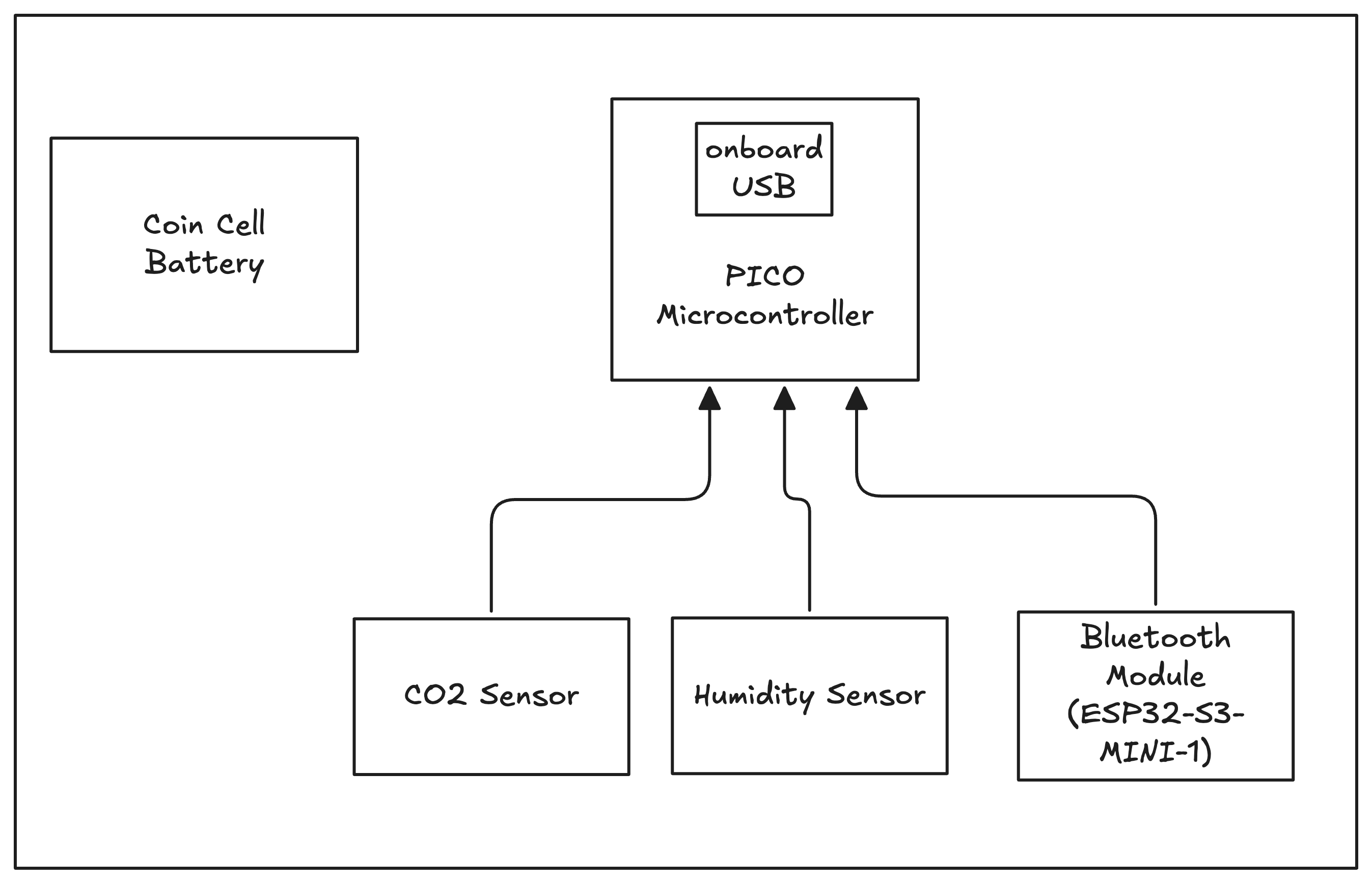 System Diagram Example 1
## Schematic Capture
In this phase we create a schematic diagram of the system and how things connect
together.
1. Using reference designs, datasheets or pre-made modules, create all the
elements of the circuit in tscircuit
2. Run design checks to make sure the circuit is hooked up correctly
In this phase you should create chip modules or [import third party chips](../guides/importing-modules-and-chips/importing-from-jlcpcb.mdx)
as you build up your circuit. You shouldn't be configuring chips in
the same file that connects all your chips together- give each chip it's own
module.
After the schematics look good, you can export to a readable netlist and upload
the netlist to AI tools like OpenAI O1 to get a review and make sure everything
is connected properly! This is also a good stage to get your schematic reviewed
by your team members.
## PCB Layout
In this phase we create a layout of the circuit on a PCB.
tscircuit automatically autoroutes the circuit for you, but you may still need
to "drag'n'drop" components in the PCB viewer to the locations you want them to
be in. Use [manual editing](../guides/tscircuit-essentials/manual-edits.mdx) to drag'n'drop
components on the PCB.
## Ordering
In this phase we order the PCB from a manufacturer. Typically this is done
by downloading [Fabrication Files](../guides/understanding-fabrication-files.md)
and "dragging and dropping" them into a manufacturer's website.
Sometimes you'll want to assemble the PCB yourself (or sometimes just a single
component that your manufacturer doesn't have!). In this case, you'll need a
lab setup to facilitate soldering.
Check out our guide on [Ordering Prototypes](./ordering-prototypes.mdx) to learn more.
---
title: Ordering Prototypes
sidebar_position: 4
description: After you've designed your device, you can use fabrication files to get your device fully assembled. The two most popular services for ordering prototypes are JLCPCB and PCBWay.
---
## Overview
After [you've designed your device](./designing-electronics-from-scratch.md),
you can use [fabrication files](../guides/understanding-fabrication-files.md)
to get your device fully assembled.
The two most popular services for
ordering prototypes are [JLCPCB](https://jlcpcb.com) and [PCBWay](https://pcbway.com).
## Ordering Through tscircuit Platform
The easiest way to order your prototypes is through the tscircuit platform, which handles the entire ordering process for you.
### Ordering Steps
Here's how the ordering process works:
### 1. Get Order Quotes
Navigate to the view packages page where you'll find the order button for your circuit.
System Diagram Example 1
## Schematic Capture
In this phase we create a schematic diagram of the system and how things connect
together.
1. Using reference designs, datasheets or pre-made modules, create all the
elements of the circuit in tscircuit
2. Run design checks to make sure the circuit is hooked up correctly
In this phase you should create chip modules or [import third party chips](../guides/importing-modules-and-chips/importing-from-jlcpcb.mdx)
as you build up your circuit. You shouldn't be configuring chips in
the same file that connects all your chips together- give each chip it's own
module.
After the schematics look good, you can export to a readable netlist and upload
the netlist to AI tools like OpenAI O1 to get a review and make sure everything
is connected properly! This is also a good stage to get your schematic reviewed
by your team members.
## PCB Layout
In this phase we create a layout of the circuit on a PCB.
tscircuit automatically autoroutes the circuit for you, but you may still need
to "drag'n'drop" components in the PCB viewer to the locations you want them to
be in. Use [manual editing](../guides/tscircuit-essentials/manual-edits.mdx) to drag'n'drop
components on the PCB.
## Ordering
In this phase we order the PCB from a manufacturer. Typically this is done
by downloading [Fabrication Files](../guides/understanding-fabrication-files.md)
and "dragging and dropping" them into a manufacturer's website.
Sometimes you'll want to assemble the PCB yourself (or sometimes just a single
component that your manufacturer doesn't have!). In this case, you'll need a
lab setup to facilitate soldering.
Check out our guide on [Ordering Prototypes](./ordering-prototypes.mdx) to learn more.
---
title: Ordering Prototypes
sidebar_position: 4
description: After you've designed your device, you can use fabrication files to get your device fully assembled. The two most popular services for ordering prototypes are JLCPCB and PCBWay.
---
## Overview
After [you've designed your device](./designing-electronics-from-scratch.md),
you can use [fabrication files](../guides/understanding-fabrication-files.md)
to get your device fully assembled.
The two most popular services for
ordering prototypes are [JLCPCB](https://jlcpcb.com) and [PCBWay](https://pcbway.com).
## Ordering Through tscircuit Platform
The easiest way to order your prototypes is through the tscircuit platform, which handles the entire ordering process for you.
### Ordering Steps
Here's how the ordering process works:
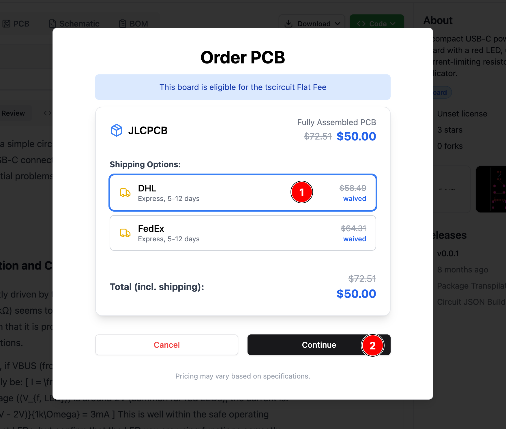
### 1. Get Order Quotes
Navigate to the view packages page where you'll find the order button for your circuit.
 The order button is present on your project's view packages page
### 2. Select Your Vendor and Quote
When you click the order button, a dialog will appear showing quotes from different vendors. Currently, JLCPCB is the only available vendor, with more vendors coming soon. Compare the prices, lead times, and shipping options, then select your preferred vendor and click continue.
The order button is present on your project's view packages page
### 2. Select Your Vendor and Quote
When you click the order button, a dialog will appear showing quotes from different vendors. Currently, JLCPCB is the only available vendor, with more vendors coming soon. Compare the prices, lead times, and shipping options, then select your preferred vendor and click continue.
 Compare quotes from multiple vendors and select the best option for your needs
### 3. Complete Your Order
Finally, you'll be redirected to a secure Stripe checkout page where you can enter your payment details and shipping address. Your PCB will be delivered directly to your specified address.
Compare quotes from multiple vendors and select the best option for your needs
### 3. Complete Your Order
Finally, you'll be redirected to a secure Stripe checkout page where you can enter your payment details and shipping address. Your PCB will be delivered directly to your specified address.
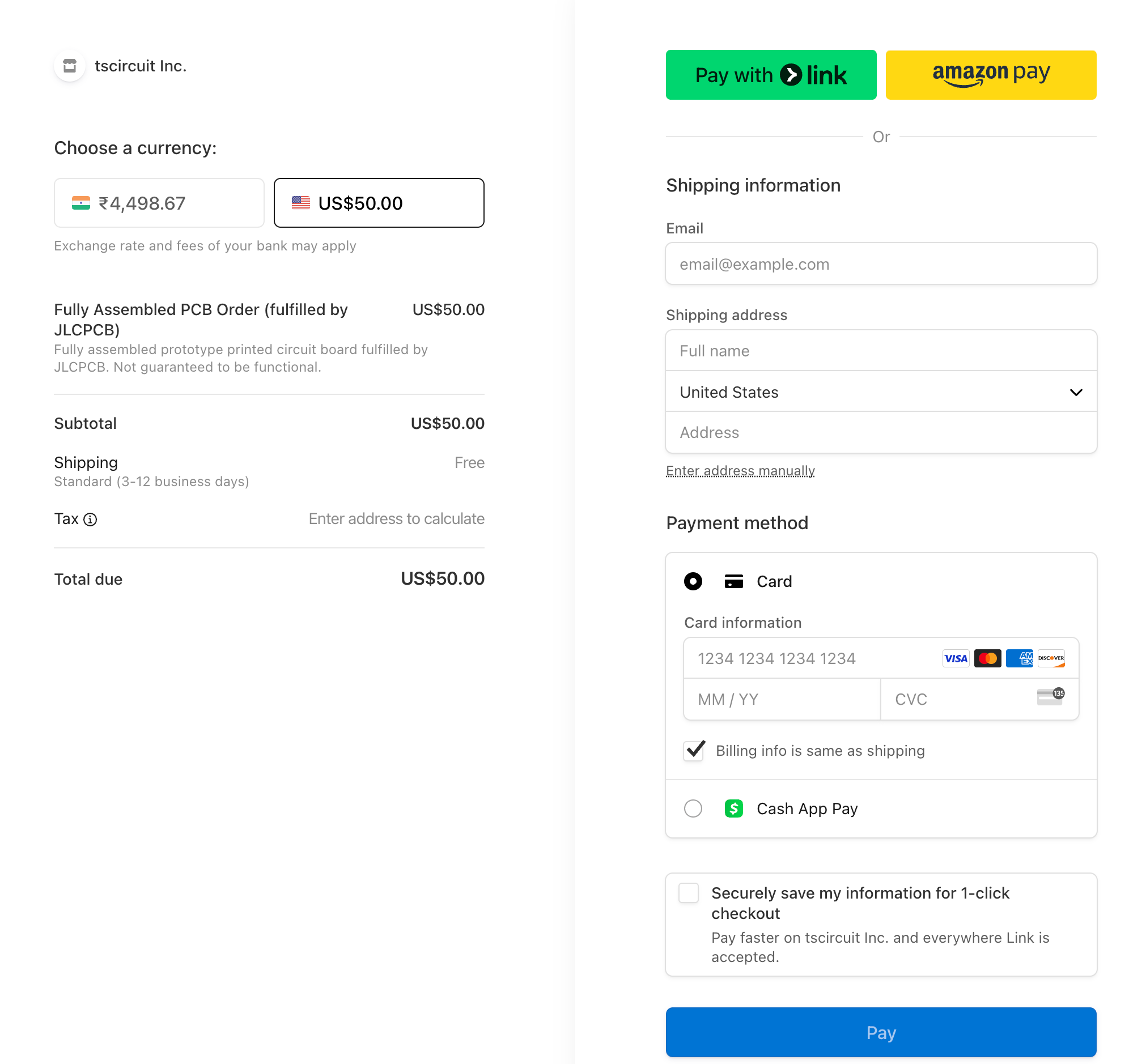 Secure checkout with Stripe handles payment and shipping details
## Uploading [Fabrication Files](../guides/understanding-fabrication-files.md)
Most fabrication or turn-key assembly services allow you to directly upload 3 types of files:
- Gerbers
- Bill of Materials (BOM CSV)
- Pick'n'Place File (CSV)
These files are all available inside your [Fabrication Files zip file](../guides/understanding-fabrication-files.md) when
you export from tscircuit.
Secure checkout with Stripe handles payment and shipping details
## Uploading [Fabrication Files](../guides/understanding-fabrication-files.md)
Most fabrication or turn-key assembly services allow you to directly upload 3 types of files:
- Gerbers
- Bill of Materials (BOM CSV)
- Pick'n'Place File (CSV)
These files are all available inside your [Fabrication Files zip file](../guides/understanding-fabrication-files.md) when
you export from tscircuit.
 Many fabricators allow you to directly drop fabrication files on their website!
## Assembling your own boards
It can sometimes be easier to assemble your own boards, this gives you more
control over your inventory and can lower the cost of your prototypes since
assembly services often have a minimum order quantity.
Even if you're assembling your own board, you should still order your PCB
from a fabrication service. PCBs require a chemical etching process to do
at home and it's rarely worth the hassle to do it yourself.
When you're assembling your own board, you can create a printout of your
Assembly View to make it easier to place components. In an assembly view,
the "pin1" location is marked with a small triangle indicator. This can help you verify
the orientation of each component as you place it.
Many fabricators allow you to directly drop fabrication files on their website!
## Assembling your own boards
It can sometimes be easier to assemble your own boards, this gives you more
control over your inventory and can lower the cost of your prototypes since
assembly services often have a minimum order quantity.
Even if you're assembling your own board, you should still order your PCB
from a fabrication service. PCBs require a chemical etching process to do
at home and it's rarely worth the hassle to do it yourself.
When you're assembling your own board, you can create a printout of your
Assembly View to make it easier to place components. In an assembly view,
the "pin1" location is marked with a small triangle indicator. This can help you verify
the orientation of each component as you place it.
 ## Controlling Part Selection
Before placing your order, there are two important component properties that affect the ordering process. The `supplierPartNumbers` prop allows you to specify exact part numbers from suppliers, helping to ensure the correct components are selected during ordering. This is particularly useful for specific or critical components.
```tsx
```
## Do Not Place Components
Components with the `doNotPlace` prop set to `true` will not be included in the parts selection for ordering. This is useful for components that you plan to solder manually or that are not available through the supplier.
```tsx
```
---
title: What are electronics made of?
sidebar_position: 1
description: >-
In this tutorial, we're going to be talking about the different elements that
make up a Printed Circuit Board (PCB). For each element, we'll show different
ways that the element can be represented in tscircuit.
---
## Overview
In this tutorial, we're going to be talking about the different elements that
make up a Printed Circuit Board (PCB). For each element, we'll show different
ways that the element can be represented in tscircuit.
## What is copper? Why are PCBs green?
Copper is a conductive material that's used on a PCB to make an electrical
connection between chips. A PCB is mostly made up of fiberglass with a small
layer of precisely etched copper. The fiberglass is non-conductive and often
coated with non-conductive green "soldermask" to cover parts of the copper that
aren't meant to be connected to chips.
## Controlling Part Selection
Before placing your order, there are two important component properties that affect the ordering process. The `supplierPartNumbers` prop allows you to specify exact part numbers from suppliers, helping to ensure the correct components are selected during ordering. This is particularly useful for specific or critical components.
```tsx
```
## Do Not Place Components
Components with the `doNotPlace` prop set to `true` will not be included in the parts selection for ordering. This is useful for components that you plan to solder manually or that are not available through the supplier.
```tsx
```
---
title: What are electronics made of?
sidebar_position: 1
description: >-
In this tutorial, we're going to be talking about the different elements that
make up a Printed Circuit Board (PCB). For each element, we'll show different
ways that the element can be represented in tscircuit.
---
## Overview
In this tutorial, we're going to be talking about the different elements that
make up a Printed Circuit Board (PCB). For each element, we'll show different
ways that the element can be represented in tscircuit.
## What is copper? Why are PCBs green?
Copper is a conductive material that's used on a PCB to make an electrical
connection between chips. A PCB is mostly made up of fiberglass with a small
layer of precisely etched copper. The fiberglass is non-conductive and often
coated with non-conductive green "soldermask" to cover parts of the copper that
aren't meant to be connected to chips.
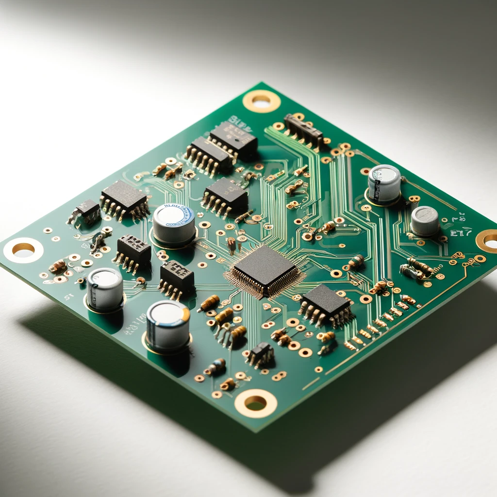 An AI-generated PCB image. All the yellow parts represent copper, while the green parts represent fiberglass with a green soldermask
A PCB can be thought of as a bunch of "printed" copper separated by fiberglass
sections that "insulate" or don't conduct electricity. We "glue" (solder) chips
to the copper "pads" to add them to the circuit.
## What are PCB layers?
When you print on a piece of paper, you can print "single-sided" or "double-sided",
PCBs can also be printed singled-sided or double-sided! The "front" of the PCB
is called the "top" layer, and the "back" of the PCB is called the "bottom" layer.
We can "print" copper to each of these layers to draw lots of wires and connect
lots of chips. Sometimes a wire needs to "go over"/"go under" another wire
because the wires aren't allowed to cross. When this happens, we can use the
"back" or "bottom layer" of the PCB to draw the wire so that the wires don't
accidentally touch.
## Vias
Vias are holes that connect different layers of PCB. Let's say you have a chip
on the top layer of a PCB and the back layer of a PCB. How can you connect them?
The copper on the top needs some way to "pass through" to the bottom layer.
This is where vias come in. A via is a hole that is "filled with copper" so that
the top layer can pass to the bottom.
An AI-generated PCB image. All the yellow parts represent copper, while the green parts represent fiberglass with a green soldermask
A PCB can be thought of as a bunch of "printed" copper separated by fiberglass
sections that "insulate" or don't conduct electricity. We "glue" (solder) chips
to the copper "pads" to add them to the circuit.
## What are PCB layers?
When you print on a piece of paper, you can print "single-sided" or "double-sided",
PCBs can also be printed singled-sided or double-sided! The "front" of the PCB
is called the "top" layer, and the "back" of the PCB is called the "bottom" layer.
We can "print" copper to each of these layers to draw lots of wires and connect
lots of chips. Sometimes a wire needs to "go over"/"go under" another wire
because the wires aren't allowed to cross. When this happens, we can use the
"back" or "bottom layer" of the PCB to draw the wire so that the wires don't
accidentally touch.
## Vias
Vias are holes that connect different layers of PCB. Let's say you have a chip
on the top layer of a PCB and the back layer of a PCB. How can you connect them?
The copper on the top needs some way to "pass through" to the bottom layer.
This is where vias come in. A via is a hole that is "filled with copper" so that
the top layer can pass to the bottom.
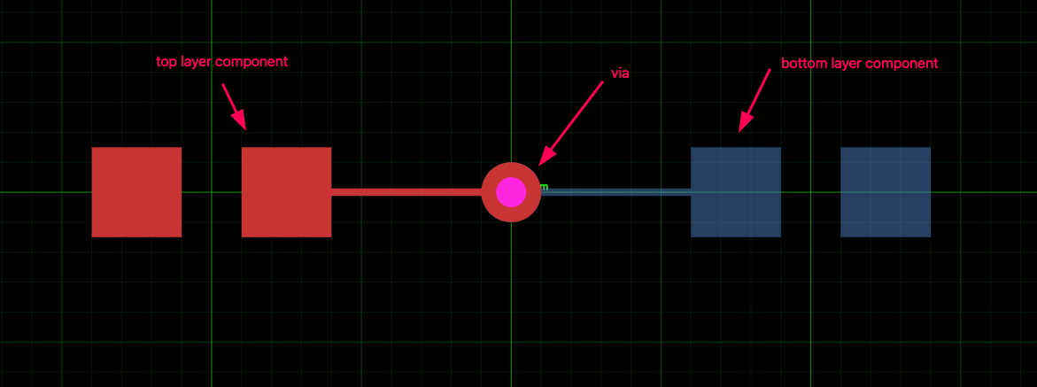 Vias connect different layers of a PCB
(
)
`} />
## Plated Holes
A plated hole is similar to a via but it's hollow so that you can push metal pins
through it. This is important for chips that have big pins that need to fit into
holes. Chips with big pins that must go through holes are called "through-hole"
chips, and chips with small
pins are called "surface-mount" chips.
(
)
`} />
## Unplated Holes "Regular Holes"
Unplated holes or "regular holes" are just holes in the printed circuit board
without any copper around them. They don't electrically connect anything, but
can be very helpful for mounting the printed circuit board.
(
)
`} />
## Traces
Traces are the wires that connect the components on a PCB. They are made of
copper and mostly covered by green soldermask so that they don't accidentally
conduct to each other if something conductive like a wire or piece of metal falls
across them.
We represent traces in PCB viewers with different colors depending on what
layer they fall on. In tscircuit, traces are always autorouted, so you don't
need to tell it which path to take- it'll automatically find one that makes sure
it doesn't cross any other traces.
Traces allow chips to "talk" to each other and for power to be shared across all
chips.
(
)
`} />
## What are inner layers?
Inner layers are layers of PCB that aren't visible, they're sandwiched on the
inside. Sometimes this is useful when you have a lot of wires to connect and
it's almost impossible to stop them from crossing each other.
Vias connect different layers of a PCB
(
)
`} />
## Plated Holes
A plated hole is similar to a via but it's hollow so that you can push metal pins
through it. This is important for chips that have big pins that need to fit into
holes. Chips with big pins that must go through holes are called "through-hole"
chips, and chips with small
pins are called "surface-mount" chips.
(
)
`} />
## Unplated Holes "Regular Holes"
Unplated holes or "regular holes" are just holes in the printed circuit board
without any copper around them. They don't electrically connect anything, but
can be very helpful for mounting the printed circuit board.
(
)
`} />
## Traces
Traces are the wires that connect the components on a PCB. They are made of
copper and mostly covered by green soldermask so that they don't accidentally
conduct to each other if something conductive like a wire or piece of metal falls
across them.
We represent traces in PCB viewers with different colors depending on what
layer they fall on. In tscircuit, traces are always autorouted, so you don't
need to tell it which path to take- it'll automatically find one that makes sure
it doesn't cross any other traces.
Traces allow chips to "talk" to each other and for power to be shared across all
chips.
(
)
`} />
## What are inner layers?
Inner layers are layers of PCB that aren't visible, they're sandwiched on the
inside. Sometimes this is useful when you have a lot of wires to connect and
it's almost impossible to stop them from crossing each other.
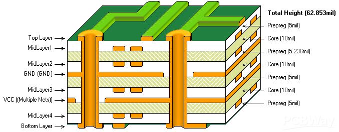 Inner layers are layers of PCB that aren't visible, they're sandwiched on the inside. Excellent image from pcbway
---
title: tsci add
description: Install tscircuit registry packages using the tsci add command
---
`tsci add` is the same as `npm add` or `bun add`, but defaults to the tscircuit
registry. If your project has the [tsci `.npmrc`](../web-apis/the-registry-api.md#using-the-tscircuit-npm-registry), you can just do `bun add @tsci/.`
and it has the same effect.
```
> tsci add seveibar/PICO_W
# Added @tsci/seveibar.PICO_W@0.0.1
```
You can then import the module and use it for your board!
(
)
`}
/>
---
title: tsci auth print-token
description: Print your current tscircuit API token for use with web services
---
`tsci auth print-token` prints your current tscircuit API token. This token can be used with the advanced web APIs such as the [Datasheet API](../web-apis/datasheet-api.md).
## Usage
```bash
tsci auth print-token
```
Make sure you have previously logged in with [`tsci login`](./tsci-login.md). The command will output a token string that you can pass in the `Authorization: Bearer ` header of API requests.
---
title: tsci build
description: Generate circuit JSON from your source files
---
`tsci build` runs the TSCircuit evaluator and writes `circuit.json` files.
## Usage
```bash
tsci build [file] [options]
```
### Arguments
- `file` *(optional)* – path to a source file or directory. If omitted, the command searches for a project entrypoint such as `index.tsx` or the `mainEntrypoint` defined in `tscircuit.config.json`. In addition, all files matching the `*.circuit.tsx` pattern are built automatically.
### Output
Output files are placed in a `dist/` directory relative to your project. Each successful build writes to its own output directory:
- `dist//circuit.json`
- `dist//pcb.svg`
- `dist//schematic.svg`
- `dist//3d.png`
For example, `src/blink.circuit.tsx` becomes `dist/src/blink/circuit.json`.
### Options
#### Error Handling
- `--ignore-errors` – do not exit with code `1` on evaluation errors.
- `--ignore-warnings` – suppress warning messages.
- `--ignore-netlist-drc` – ignore netlist DRC errors and warnings.
- `--ignore-pin-specification-drc` – ignore pin-specification DRC errors and warnings.
- `--ignore-placement-drc` – ignore placement DRC errors and warnings.
- `--ignore-routing-drc` – ignore routing DRC errors and warnings.
- `--ignore-config` – ignore options from `tscircuit.config.json`.
#### Build Control
- `--ci` – run install and optional prebuild/build commands (or default CI build).
- `--disable-pcb` – disable PCB outputs.
- `--routing-disabled` – disable routing during circuit generation.
- `--disable-parts-engine` – disable the parts engine.
- `--concurrency ` – number of files to build in parallel (default: 1).
#### Output Formats
##### Images & 3D Models
- `--preview-images` – generate images for one selected build output.
- `--all-images` – generate images for every successful build output.
- `--pngs` – generate PNG outputs during build generation.
- `--pcb-png` – generate PCB PNG outputs during build generation.
- `--svgs` – generate both `pcb.svg` and `schematic.svg`.
- `--pcb-svgs` – generate only `pcb.svg`.
- `--schematic-svgs` – generate only `schematic.svg`.
- `--3d-png` – generate `3d.png`.
- `--3d` – alias for `--3d-png`.
- `--pcb-only` – generate only `pcb.svg` from the selected SVG outputs.
- `--schematic-only` – generate only `schematic.svg` from the selected SVG outputs.
- `--preview-gltf` – generate a GLTF file from the preview entrypoint.
- `--glbs` – generate GLB 3D model files for every successful build output.
- `--show-courtyards` – show courtyard outlines in PCB SVG outputs.
##### KiCad Export
- `--kicad-project` – generate KiCad project directories (`.kicad_sch`, `.kicad_pcb`, `.kicad_pro`) for each successful build output.
- `--kicad-project-zip` – generate a zipped KiCad project for each successful build output.
- `--kicad-library` – generate KiCad symbol/footprint library in `dist/kicad-library`.
- `--kicad-library-name ` – specify the name of the KiCad library.
- `--kicad-pcm` – generate KiCad PCM (Plugin and Content Manager) assets in `dist/pcm`.
##### Diagnostics
- `--profile` – log per-circuit `circuit.json` generation time during build.
##### Library & Site Generation
- `--transpile` – transpile the entry file to JavaScript for use as a library.
- `--site` – generate a static site in the dist directory.
- `--use-cdn-javascript` – use CDN-hosted JavaScript instead of bundled standalone file for `--site`.
##### Injecting Props
- `--inject-props ` – inject JSON props into the built file's default export.
- `--inject-props-file ` – load injected props JSON from a file.
### Targeting specific sources
- `tsci build path/to/file.circuit.tsx` – builds the given file, even if it does not match the `includeBoardFiles` glob in `tscircuit.config.json`.
- `tsci build path/to/directory` – scans only the files inside `path/to/directory` that both satisfy the `includeBoardFiles` glob and reside within the directory. Files outside the directory or filtered out by the glob are skipped.
Use this command before publishing or in CI to ensure your circuits evaluate correctly.
## Image generation behavior
`--preview-images` and `--all-images` choose which build outputs receive images:
- `--preview-images` writes image files for one selected build.
- `--all-images` writes image files for every successful build.
The image selection flags choose which files are written for each selected build:
- If you do not pass any image selection flags, the default image set is `pcb.svg`, `schematic.svg`, and `3d.png`.
- If you pass any image selection flags, those flags explicitly control which files are written.
- `--pcb-only` and `--schematic-only` filter SVG outputs.
- `--3d` can be combined with the newer flags and adds `3d.png`.
- Use the image selection flags with either `--preview-images` or `--all-images`.
Preview target selection uses this precedence:
1. `previewComponentPath`
2. `mainEntrypoint`
3. The first successful build
## Output Directory Structure
When using various build options, the output structure looks like:
```text
dist/
├── my-circuit/
│ ├── circuit.json # Always generated for that build output
│ ├── pcb.svg # With --preview-images/--all-images, --svgs, --pcb-svgs, etc.
│ ├── schematic.svg # With --preview-images/--all-images, --svgs, --schematic-svgs, etc
│ ├── 3d.png # With --preview-images/--all-images, --pngs, or --3d
│ ├── 3d.glb # With --glbs
│ └── kicad/
│ ├── my-circuit.kicad_sch # With --kicad-project
│ ├── my-circuit.kicad_pcb # With --kicad-project
│ └── my-circuit.kicad_pro # With --kicad-project
├── my-circuit.gltf # With --preview-gltf (preview entrypoint only)
├── kicad-library/ # With --kicad-library
├── pcm/ # With --kicad-pcm
├── index.html # With --site
├── standalone.min.js # With --site (unless --use-cdn-javascript)
├── index.js # With --transpile
├── index.cjs # With --transpile
└── index.d.ts # With --transpile
```
## Transpiling circuit entrypoints
Pass the `--transpile` flag when you want your codebase to be a reusable module that can be imported into other projects. Your "entrypoint", usually `lib/index.tsx` will be the source for the bundle. Export any circuits you'd like out of that file
- `dist//index.js` – an ESM bundle
- `dist/.cjs` – a CommonJS bundle
- `dist/.d.ts` – generated type declarations that reflect the JSX surface of your entry file
### Example project
Spin up a scratch directory with `tsci init` to reproduce the transpile flow locally:
```bash
mkdir tsci-transpile-demo
cd tsci-transpile-demo
tsci init
```
Replace the generated `index.tsx` with a tiny RC circuit:
```tsx title="index.tsx"
import React from "react"
export default () => (
)
```
Then run the transpile build:
```bash
tsci build --transpile
```
The build writes `dist/index/circuit.json` as usual, then finishes by bundling the entrypoint and printing the paths to the emitted ESM, CJS, and type declaration artifacts.
```text
dist
├── index
│ └── circuit.json
├── index.cjs
├── index.d.ts
└── index.js
2 directories, 4 files
```
---
title: tsci check
description: Partially build and validate circuit artifacts
---
`tsci check` partially builds your circuit and validates specific aspects of the output. It is useful for catching issues early without running a full build.
## Usage
```bash
tsci check [options]
```
## Subcommands
### `tsci check netlist`
Partially build and validate the netlist.
```bash
tsci check netlist [refdeses]
```
- `refdeses` *(optional)* – reference designators to scope the check (e.g. `R1 C1`)
### `tsci check placement`
Partially build and validate component placement.
```bash
tsci check placement [refdeses]
```
- `refdeses` *(optional)* – reference designators to scope the check
### `tsci check routing`
Partially build and validate the routing.
```bash
tsci check routing
```
:::note
These subcommands are currently under development and may not be fully implemented yet.
:::
---
title: tsci clone
description: Clone a package from the tscircuit registry to your local machine
---
`tsci clone` downloads a package from the [tscircuit registry](https://tscircuit.com/trending) into a local directory so you can inspect, modify, or build on top of it.
## Usage
```bash
tsci clone [package] [options]
```
### Arguments
- `package` – package identifier in one of these forms:
- `author/packageName`
- `@tsci/author.packageName`
- `https://tscircuit.com/author/packageName`
### Options
- `-a, --include-author` – include the author name in the directory path (creates `author.packageName/` instead of `packageName/`)
- `--bug-report ` – clone a bug report project instead of a regular package
## Examples
Clone a package by name:
```bash
tsci clone seveibar/PICO_W
```
Clone using a URL:
```bash
tsci clone https://tscircuit.com/seveibar/PICO_W
```
Clone with the author prefix in the directory name:
```bash
tsci clone seveibar/PICO_W --include-author
# Creates seveibar.PICO_W/
```
Clone a bug report:
```bash
tsci clone --bug-report abc123
```
## Configuration
You can set the `alwaysCloneWithAuthorName` config key to always include the author name without passing `-a`:
```bash
tsci config set alwaysCloneWithAuthorName true
```
---
title: tsci config
description: Manage tscircuit CLI configuration
---
`tsci config` lets you view and modify tscircuit CLI configuration values. There are two types of configuration: **global** CLI settings and **project-specific** settings stored in `tscircuit.config.json`.
## Subcommands
### `tsci config print`
Print the current global CLI configuration as JSON.
```bash
tsci config print
```
### `tsci config set`
Set a configuration value.
```bash
tsci config set
```
#### Global Configuration Keys
| Key | Type | Description |
|-----|------|-------------|
| `alwaysCloneWithAuthorName` | boolean | Always include author name when cloning packages |
#### Project Configuration Keys
These keys are saved to `tscircuit.config.json` in your project directory:
| Key | Description |
|-----|-------------|
| `mainEntrypoint` | Path to the main circuit entrypoint file |
| `kicadLibraryEntrypointPath` | Path to the KiCad library entrypoint |
| `previewComponentPath` | Path to the preview component |
| `siteDefaultComponentPath` | Default component for static site generation |
| `prebuildCommand` | Command to run before building |
| `buildCommand` | Custom build command |
## Examples
```bash
# Always include author in clone directory names
tsci config set alwaysCloneWithAuthorName true
# Set the project entrypoint
tsci config set mainEntrypoint lib/index.tsx
# View current config
tsci config print
```
---
title: tsci convert
description: Convert a KiCad footprint file to a tscircuit component
---
`tsci convert` takes a `.kicad_mod` footprint file and converts it into a tscircuit TSX component, making it easy to reuse existing KiCad footprints in your tscircuit projects.
## Usage
```bash
tsci convert [options]
```
### Arguments
- `file` *(required)* – path to the `.kicad_mod` file
### Options
- `-o, --output ` – output TSX file path (defaults to the same directory as the input file)
- `-n, --name ` – component name for the export (defaults to the input filename without extension)
## Examples
Convert a footprint using defaults:
```bash
tsci convert MyFootprint.kicad_mod
# Creates MyFootprint.tsx in the same directory
```
Convert with a custom component name and output path:
```bash
tsci convert MyFootprint.kicad_mod --name CustomPad --output src/components/CustomPad.tsx
```
---
title: tsci dev
description: Run a local preview server for your tscircuit project
sidebar_position: 2
---
`tsci dev` runs a web server that lets you see a preview of your electronics
in your web browser.
## Usage
```bash
tsci dev [file] [options]
```
### Arguments
- `file` *(optional)* – path to a package file or directory
### Options
- `-p, --port ` – port to run the server on (default: `3020`)
- `--kicad-pcm` – enable KiCad PCM proxy server at `/pcm/*`
After you run `tsci dev` you should see a preview of your entrypoint file in
your web browser on http://localhost:3020


## KiCad PCM Server
The `--kicad-pcm` flag starts a KiCad Plugin and Content Manager (PCM) server in
the background alongside the development server. This allows you to install your
tscircuit components directly into KiCad as a library.
```bash
tsci dev --kicad-pcm
```
Example output:
```
➜ library tsci dev --kicad-pcm
@tscircuit/cli@0.1.851 ready in 1067ms
➜ Local: http://localhost:3023/#file=lib%2Findex.ts
Watching "my-project" for changes...
➜ Auto-updating KiCad PCM Server: http://localhost:3023/pcm/repository.json
```
### Adding the PCM Repository to KiCad
To use your tscircuit components in KiCad:
1. Open KiCad and go to **Plugin and Content Manager**
2. Click **Manage Repositories**
3. Click the **Add** button (plus icon)
4. Enter the PCM URL shown in your terminal (e.g., `http://localhost:3023/pcm/repository.json`)
5. Click **OK** to save

Once added, your tscircuit library will appear in KiCad's Plugin and Content
Manager. The library automatically updates as you make changes to your tscircuit
project, so you can iterate on your designs without needing to re-export.
---
title: tsci doctor
description: Run diagnostic checks for your tscircuit setup
---
`tsci doctor` runs a series of diagnostic checks to verify that your local tscircuit development environment is set up correctly. Use it to troubleshoot issues with your configuration, dependencies, or authentication.
## Usage
```bash
tsci doctor
```
The command will print the status of each check and highlight any problems it finds.
---
title: tsci export
description: Export tscircuit files to various formats including SVG schematics, PCB layouts, and fabrication files.
---
import ImageWithCaption from "../../src/components/ImageWithCaption"
## Overview
`tsci export` can be used to convert a `tsx` file or `circuit.json` file into
various output formats including schematics, PCB layouts, fabrication files, and more.
## Usage
```bash
tsci export [options]
```
### Arguments
- ``: Path to the source file (`.tsx` or `.circuit.json`)
### Options
- `-f, --format `: Output format (defaults to "json")
- `-o, --output `: Custom output file path
- `--disable-parts-engine`: Disable the parts engine during circuit evaluation
- `--show-courtyards`: Show courtyard outlines in PCB SVG output
## Supported Formats
The following export formats are supported:
| Format | Description |
|--------|-------------|
| `json` | Circuit JSON format (alias for `circuit-json`) |
| `circuit-json`| Circuit JSON format |
| `schematic-svg` | Schematic view as SVG |
| `pcb-svg` | PCB layout as SVG |
| `assembly-svg` | Assembly view as SVG |
| `gerbers` | Gerber fabrication files (zipped) |
| `readable-netlist` | Human-readable netlist |
| `specctra-dsn` | Specctra DSN format for autorouting |
| `gltf` | Text-based 3D scene (glTF 2.0) that references board meshes and textures |
| `glb` | Binary glTF bundle that packs geometry, materials, and textures into a single file |
| `step` | STEP 3D model (ISO-10303-21) for high-fidelity CAD integration |
| `kicad_sch` | KiCad schematic file |
| `kicad_pcb` | KiCad PCB layout file |
| `kicad_zip` | Zipped KiCad project (schematic + PCB) |
| `kicad-library` | KiCad library with symbols, footprints, and 3D models (see [Exporting KiCad Library](../guides/kicad/exporting-kicad-library.md)) |
| `spice` | SPICE netlist with simulation results exported as `.spice.cir` and `.csv` |
## Examples
Export to circuit JSON:
```bash
tsci export circuit.tsx
```
Export as schematic SVG:
```bash
tsci export circuit.tsx -f schematic-svg
```
Export as assembly SVG:
```bash
tsci export circuit.tsx -f assembly-svg
```
Export PCB layout with custom output path:
```bash
tsci export circuit.tsx -f pcb-svg -o my-pcb-layout.svg
```
Export PCB SVG with courtyard outlines:
```bash
tsci export circuit.tsx -f pcb-svg --show-courtyards
```
Export to Specctra DSN format:
```bash
tsci export circuit.tsx -f specctra-dsn
```
## Exporting 3D models
Use the `gltf`, `glb`, or `step` formats when you want a 3D representation of your board for use in CAD tools, AR viewers, or when embedding on the web.
### Export as glTF
```bash
tsci export circuit.tsx --format gltf
```
This produces a `.gltf` file (plus any referenced texture files) that follows the [glTF 2.0](https://www.khronos.org/gltf/) spec. Because the assets stay separate, glTF exports are easier to diff in git and you can selectively optimize textures.
### Export as GLB
```bash
tsci export circuit.tsx --format glb
```
The `glb` format wraps the same data into a single binary so you can upload one file to a web viewer (for example, https://gltf.report/ or `model-viewer`). This is handy for sharing previews or attaching a lightweight CAD model to a manufacturing request.
Both commands work with `.tsx` source files as well as `.circuit.json` files, so you can export whichever representation you already have. Each command writes the 3D model next to the input file unless you override the location with `--output `.
### Export as STEP
```bash
tsci export circuit.tsx --format step
```
This produces a `.step` file that can be imported into most mechanical CAD tools.
## Output Files
By default, the exported file will be saved in the same directory as the input file, with a filename based on the input filename and the chosen format. For example:
- Input: `my-circuit.tsx`
- Format: `pcb-svg`
- Default output: `my-circuit-pcb.svg`
You can override the output location using the `-o` or `--output` option.
---
title: tsci import
description: Search JLCPCB or the tscircuit registry and import a component into your project
---
`tsci import` searches for components across JLCPCB and the tscircuit registry, then lets you interactively select and install one into your project. It is a convenient way to discover and add parts without leaving the terminal.
## Usage
```bash
tsci import [options]
```
### Arguments
- `query` *(required)* – chip name, part number, or package name to search for
### Options
- `--jlcpcb` – search JLCPCB components only
- `--lcsc` – alias for `--jlcpcb`
- `--tscircuit` – search tscircuit registry packages only
- `--download` – download JLCPCB 3D model assets (`.obj` and `.step` files) and reference them locally in the component
When no filter options are provided, both JLCPCB and the tscircuit registry are searched.
## Examples
Search everywhere and pick a component interactively:
```bash
$ tsci import "ESP32-S3"
✔ Select a part to import › seveibar/esp32-s3-mini-1-n8 - Generated from JLCPCB part number C2913206
⠋ Installing seveibar/esp32-s3-mini-1-n8...Adding @tsci/seveibar.esp32-s3-mini-1-n8...
> bun add @tsci/seveibar.esp32-s3-mini-1-n8
bun add v1.3.3 (274e01c7)
installed @tsci/seveibar.esp32-s3-mini-1-n8@0.1.0
1 package installed [1.91s]
✓ Added @tsci/seveibar.esp32-s3-mini-1-n8 successfully
✔ Installed seveibar/esp32-s3-mini-1-n8
```
Search only JLCPCB:
```bash
$ tsci import "C16040" --jlcpcb
✔ Imported /home/rushabh/testing/imports/MCP4822_E_SN.tsx
```
Download 3D model assets (.obj and .step) alongside the component:
```bash
$ tsci import "C2934569" --jlcpcb --download
✔ Imported imports/ESP32_C3_MINI_1_H4/ESP32_C3_MINI_1_H4.tsx
```
Search only the tscircuit registry:
```bash
$ tsci import "usb-c" --tscircuit
✔ Select a part to import › seveibar/smd-usb-c
⠋ Installing seveibar/smd-usb-c...Adding @tsci/seveibar.smd-usb-c...
> bun add @tsci/seveibar.smd-usb-c
bun add v1.3.3 (274e01c7)
installed @tsci/seveibar.smd-usb-c@0.0.2
1 package installed [18.02s]
✓ Added @tsci/seveibar.smd-usb-c successfully
✔ Installed seveibar/smd-usb-c
```
After selecting a component, `tsci import` will automatically install it into your project.
---
title: tsci init
sidebar_position: 0
description: Initialize a new TSCircuit project
---
`tsci init` bootstraps a fresh project in the current directory. It creates the
basic files needed to start developing a board, including:
- `index.tsx` – your main circuit entrypoint
- `package.json` with the required dependencies
- `tsconfig.json`
- `.gitignore` and other configuration files
You can run the command interactively or pass `-y` to accept all defaults.
### Options
- `-y, --yes` – use defaults and skip prompts
- `--no-install` – skip installing dependencies after initialization
```bash
mkdir my-circuit
cd my-circuit
# Initialize with prompts
tsci init
# or skip prompts
tsci init -y
# skip dependency installation
tsci init -y --no-install
```
After initialization you will see a directory structure similar to the following:
```text
my-circuit/
├─ index.tsx
├─ package.json
├─ tsconfig.json
└─ tscircuit.config.json
```
import tsciInitImage from "../../static/img/tsci-init.png";
import ImageWithCaption from "../../src/components/ImageWithCaption";
Next, run `tsci dev` to start the development server and view your circuit in the
browser.
---
title: tsci install
description: Install project dependencies or a specific package
---
`tsci install` installs all project dependencies when called without arguments, or installs a specific package when given a package specifier. It supports npm packages, GitHub URLs, and KiCad libraries.
## Usage
```bash
tsci install [packageSpec]
```
### Arguments
- `packageSpec` *(optional)* – a package to install. Can be an npm package name, a GitHub URL, or a KiCad library URL. When omitted, installs all project dependencies.
## Examples
Install all project dependencies:
```bash
$ tsci install
Found existing package.json.
Installing dependencies using bun...
> bun install
bun install v1.3.3 (274e01c7)
Checked 307 installs across 338 packages (no changes) [121.00ms]
Dependencies installed successfully.
```
Install a specific package from a GitHub URL:
```bash
tsci install https://github.com/espressif/kicad-libraries
```
---
title: tsci login
description: Sign in to the tscircuit registry to enable publishing and cloud tools
sidebar_position: 1
---
`tsci login` allows you to login to the tscircuit registry. You don't need to
login to tscircuit to use any tools, but logging in does enable the following
great features:
- Cloud Autorouting (`autorouter="auto-cloud"`)
- Package Management (publishing and automatic bundling)
:::info
You don't need a tscircuit account to download and use other people's packages
:::
`tsci login` will take you to a login page where you'll sign in with Github.
After the login flow you'll have have token on your machine that authenticates
you to publish packages or use the cloud autorouter.
## Logout
To logout again, just run `tsci logout`
## Other Auth Functions
Run `tsci auth --help` to see all available auth subcommands.
### `tsci auth whoami`
Show information about the currently authenticated user, including your tscircuit handle, email, account ID, and session details.
```bash
tsci auth whoami
```
### `tsci auth set-token`
Manually set your authentication token (must be a valid JWT).
```bash
tsci auth set-token
```
### `tsci auth setup-npmrc`
Configure your global `.npmrc` file with authentication for tscircuit private packages. You must be logged in first.
```bash
tsci auth setup-npmrc
```
See also: [`tsci auth print-token`](./tsci-auth-print-token.md) for printing your token for use with the [Registry API](../web-apis/the-registry-api.md).
---
title: tsci push
sidebar_position: 2
description: |
tsci push uploads your package to the tscircuit registry for module re-use
---
tscircuit code, like React code, is distributed as a "package". `tsci push` uploads your package to the [tscircuit registry](https://tscircuit.com/trending) to enable sharing with your team.
After publishing, you can use the [tsci add](https://docs.tscircuit.com/command-line/tsci-add) command to install your package as part of a larger circuit.
## Usage
```bash
tsci push [options]
```
## Options
- `--compress` – Compresses the payload before upload. This is useful for large projects and slower connections because it reduces upload size.
After running `tsci push` you can see your package on your tscircuit registry page. Packages default to private visibility, but you can change this from your registry page to enable sharing your package with the broader ecosystem.
import tsciPushImage from "../../static/img/tsci-push.png"
import registrySnippetImage from "../../static/img/registry-snippet.png"
import ImageWithCaption from "../../src/components/ImageWithCaption";
---
title: tsci remove
description: Remove a tscircuit package from your project
---
`tsci remove` removes a tscircuit package from your project, the inverse of [`tsci add`](./tsci-add.mdx).
## Usage
```bash
tsci remove
```
### Arguments
- `package` *(required)* – the package to remove (e.g. `author/package-name`)
## Example
```bash
$ tsci remove seveibar/PICO_W
# Removing @tsci/seveibar.PICO_W...
# Removed @tsci/seveibar.PICO_W successfully.
```
---
title: tsci search
description: Discover footprints and packages across the tscircuit ecosystem
---
`tsci search` finds footprints and packages from across the tscircuit ecosystem.
### Options
- `--kicad` – search KiCad footprints
- `--jlcpcb` – search JLCPCB components
- `--lcsc` – alias for `--jlcpcb`
- `--tscircuit` – search tscircuit registry packages
- `--json` – output search results as JSON
When no filter options are provided, all sources are searched.
## Usage
```bash
$ tsci search resistor
Found 10 footprint(s) from KiCad:
1. Resistor_SMD/R_01005_0402Metric_Pad0.57x0.30mm_HandSolder
2. Resistor_SMD/R_01005_0402Metric
3. Resistor_SMD/R_0201_0603Metric_Pad0.64x0.40mm_HandSolder
4. Resistor_SMD/R_0201_0603Metric
5. Resistor_SMD/R_0402_1005Metric_Pad0.72x0.64mm_HandSolder
6. Resistor_SMD/R_0402_1005Metric
7. Resistor_SMD/R_0603_1608Metric_Pad0.98x0.95mm_HandSolder
8. Resistor_SMD/R_0603_1608Metric
9. Resistor_SMD/R_0612_1632Metric_Pad1.18x3.40mm_HandSolder
10. Resistor_SMD/R_0612_1632Metric
Found 11 package(s) in the tscircuit registry:
1. seveibar/usb-c-flashlight (vundefined) - Stars: 5 - A compact USB-C powered push button board with a red LED, utilizing a single current-limiting resistor for the LED indicator.
2. ArnavK-09/OPT4048DTSR (vundefined) - Stars: 3 - Sparkfun schematic with an 8-pin SOIC-8 IC (OPT4048) connected to a 3.3V power supply, ground, I2C bus lines (SCL, SDA), an address pin, an interrupt pin, plus a pull-up resistor and a decoupling capacitor.
...
```
Use any search term to discover related footprints or published projects.
### JSON Output Example
You can output search results as JSON by using the `--json` flag.
```bash
$ tsci search --jlcpcb "RP2040" --json
```
```json
{
"query": "RP2040",
"results": [
{
"source": "jlcpcb",
"lcsc": 2040,
"mfr": "RP2040",
"package": "LQFN-56(7x7)",
"is_basic": false,
"is_preferred": false,
"description": "",
"stock": 42449,
"price": 0.872857143
},
{
"source": "jlcpcb",
"lcsc": 5350143,
"mfr": "RP2040-Zero",
"package": "-",
"is_basic": false,
"is_preferred": false,
"description": "",
"stock": 51,
"price": 5.091428571
}
]
}
```
---
title: tsci simulate
description: Run circuit simulations from the command line
---
`tsci simulate` runs circuit simulations on your tscircuit designs. Currently it supports analog SPICE simulations.
## Usage
```bash
tsci simulate [options]
```
## Subcommands
### `tsci simulate analog`
Run an analog SPICE simulation on a circuit file.
```bash
tsci simulate analog [options]
```
#### Arguments
- `file` *(required)* – path to a tscircuit `.tsx` or `.circuit.json` file
#### Options
- `--disable-parts-engine` – disable the parts engine during circuit evaluation
The command generates a SPICE netlist from your circuit, runs the simulation, and prints the results in a table format.
## Example
```bash
$ tsci simulate analog my-circuit.circuit.tsx
ngspice 1 -> ngspice 1 ->
Note: No compatibility mode selected!
Circuit: * circuit json to spice netlist
ngspice 2 -> Doing analysis at TEMP = 27.000000 and TNOM = 27.000000
Using SPARSE 1.3 as Direct Linear Solver
Operating point simulation skipped by 'uic',
now using transient initial conditions.
No. of Data Rows : 1011
ngspice 3 -> binary raw file "out.raw"
Index time v(n1) v(n2) v(vp_in1) i(vsimulation_voltage_source_0)
0 1.000000e-6 6.283184e-4 6.283184e-4 1.256637e-3 -1.742483e-15
1 2.000000e-6 1.256637e-3 1.256637e-3 2.513274e-3 -3.485349e-15
2 4.000000e-6 2.513273e-3 2.513273e-3 5.026547e-3 -6.972993e-15
3 8.000000e-6 5.026544e-3 5.026544e-3 1.005309e-2 -1.396437e-14
4 1.600000e-5 1.005307e-2 1.005307e-2 2.010614e-2 -2.807686e-14
5 3.200000e-5 2.010598e-2 2.010598e-2 4.021195e-2 -5.737260e-14
```
---
title: tsci transpile
description: Transpile TypeScript/TSX to JavaScript for distribution as a reusable library
---
`tsci transpile` converts your TypeScript/TSX circuit files into distributable JavaScript bundles (ESM, CommonJS, and type declarations). This is useful when you want to publish your circuit as a reusable module.
## Usage
```bash
tsci transpile [file]
```
### Arguments
- `file` *(optional)* – path to the entry file. If omitted, the command uses the detected entrypoint (same logic as `tsci build`).
## Output
The transpile command generates three files in the `dist/` directory:
| File | Format |
|------|--------|
| `index.js` | ESM bundle |
| `index.cjs` | CommonJS bundle |
| `index.d.ts` | TypeScript type declarations |
:::tip
`tsci transpile` is equivalent to running `tsci build --transpile` without the circuit JSON generation step. Use `tsci build --transpile` when you want both `circuit.json` and the transpiled output.
:::
---
title: Sponsorships
description: Understand how tscircuit contributor sponsorships are awarded
---
tscircuit automatically sponsors regular contributors based on the impact of
their work. This activity is tracked in the open-source
[contribution-tracker](https://github.com/tscircuit/contribution-tracker),
which powers [contributions.tscircuit.com](https://contributions.tscircuit.com)
and resets every Wednesday.
## How the contribution tracker works
- Every PR across the tscircuit GitHub org is scanned and summarized via an LLM
so we can consistently understand the scope of each change.
- The LLM classifies each diff/PR into attributes such as **🐳 Major**,
**🐙 Minor**, and **🐌 Tiny** impact levels and assigns a star rating that feeds
the weekly score shown on the sponsorship leaderboard.
- The resulting data is organized into the sections you see on the tracker—such
as Contributor Overview, PRs by Repository, and PRs by Contributor—so you can
quickly understand where impactful work is happening across the ecosystem.
- Historical exports, including weekly contribution overviews and AI-generated
monthly changelogs, are kept directly in the
[contribution-tracker repo](https://github.com/tscircuit/contribution-tracker)
if you want to dig deeper into past activity.
**The best way to increase sponsorship eligibility is to consistently contribute
high-impact improvements.** A great approach is to actively use tscircuit,
report confusing or buggy behavior, and submit fixes for the issues you uncover.
Contributors who repeatedly do this tend to build deep product context and
deliver meaningful improvements over time.
## How sponsorship amounts are calculated
Sponsorship payouts are based on the last four weeks of star ratings captured by
the tracker. The algorithm takes the median, minimum, and maximum weekly star
counts to decide on a base amount—ranging from $15 for occasional stars up to
$500 for consistently high-impact weeks—with a $5 safety net for anyone whose
historical high score stays above 3. You can read the current logic directly in
[`getSponsorshipAmount.ts`](https://github.com/tscircuit/contribution-tracker/blob/main/lib/scoring/getSponsorshipAmount.ts)
for the exact thresholds.
Maintainers receive an additional fixed monthly sponsorship on top of the weekly
calculation so their support stays stable. Those maintainer bonuses are defined
alongside the algorithm in the tracker codebase.
To be eligible for Github Sponsorship, you must be in a supported country and
have Github Sponsors enabled on your Github profile.
---
title: Contributing Autorouting Datasets
description: Guidelines for naming, structuring, visualizing, and contributing autorouting datasets.
---
Autorouting datasets help develop new features for specific cases. If you are
running into an autorouter issue, you may be able to generate a dataset: start
with a `tsci init` project, create samples that replicate the issue, and put the
dataset into a repo that can be tested directly with our autorouter.
## Start from an existing dataset
Before creating a new repository, inspect the latest dataset in the same family
and copy its structure. These repos are good bootstrapping references:
- [`tscircuit/dataset-srj19`](https://github.com/tscircuit/dataset-srj19)
for a generated Simple Route JSON dataset with a Cosmos sample viewer.
- [`tscircuit/dataset-srj18`](https://github.com/tscircuit/dataset-srj18)
for a dataset generated from KiCad boards.
- [`tscircuit/tscircuit-autorouter`](https://github.com/tscircuit/tscircuit-autorouter)
for the current autorouter benchmark integration.
Use the [Simple Route JSON reference](../advanced/simple-route-json.mdx) when
you need field-level details for `bounds`, `obstacles`, `connections`, layers,
and traces.
## Name the dataset
Use the
[Dataset Naming Guidelines](https://github.com/tscircuit/handbook/blob/main/guides/dataset-guidelines.md#dataset-naming-guidelines)
for dataset naming conventions. In brief, increase the number from the latest
known dataset in the same prefix and use two digits, such as `01`, `02`, or
`19`.
## Keep the package GitHub-installable
Dataset packages should install directly from GitHub because the autorouter pins
dataset dependencies to repository commits. Follow the
[Dataset Library Structure](https://github.com/tscircuit/handbook/blob/main/guides/dataset-guidelines.md#dataset-library-structure)
guidance, then compare your package structure against the reference dataset
repos above.
If the dataset starts from Circuit JSON, follow
[Creating Simple Route JSON from Circuit JSON](https://github.com/tscircuit/handbook/blob/main/guides/dataset-guidelines.md#creating-simple-route-json-from-circuit-json).
The [`dataset-srj18` README](https://github.com/tscircuit/dataset-srj18) shows
that flow for KiCad-derived samples.
## Add a visualization
Every dataset should have a way to inspect samples before running a benchmark.
Use the
[React Visualizers/Debuggers](https://github.com/tscircuit/handbook/blob/main/guides/bootstrapping-repos.md#react-visualizersdebuggers)
guide for the Cosmos sample viewer pattern. The
[`dataset-srj19`](https://github.com/tscircuit/dataset-srj19)
repo is a good public example of a dataset with a viewer.
## Add snapshot tests
Use the
[Dataset Guidelines](https://github.com/tscircuit/handbook/blob/main/guides/dataset-guidelines.md)
for the dataset structure, then include at least one representative test so
changes to generated Simple Route JSON or visualization output are easy to
review.
## Add the dataset to autorouter benchmarks
After the dataset repository is usable on its own, add a follow-up change to
[`tscircuit/tscircuit-autorouter`](https://github.com/tscircuit/tscircuit-autorouter)
so router contributors can run the dataset locally.
After integration, the dataset should appear in the autorouter benchmark list.
Add the benchmark integration in this order:
1. Pin the dataset in `package.json` using a GitHub URL and commit hash.
2. If TypeScript cannot infer the dataset package types, add a module shim in
`types/dataset-module-shims.d.ts`.
3. Add the dataset to `scripts/benchmark/scenarios.ts`: include its short name
in `DATASET_NAMES`, add aliases, add a loader, add the scenario key pattern,
and update `DATASET_OPTIONS_LABEL`.
4. Follow the
[`benchmark.sh` guide](https://github.com/tscircuit/handbook/blob/main/guides/benchmark-sh.md)
while updating `benchmark.sh` help text and dataset parsing so contributors
can run the dataset with `./benchmark.sh --dataset `.
5. Add or update benchmark coverage so `--dataset ` works
consistently in `benchmark.sh`, `scripts/benchmark/scenarios.ts`, and
`run-sample.sh`.
6. Run one targeted sample and a small benchmark with the dataset name you added
before opening the PR.
If the dataset captures a reported autorouter bug, also read
[Report Autorouter Bugs](./report-autorouter-bugs.md). The autorouter repo has
helpers for turning bug reports into fixtures and snapshot tests.
---
title: Getting Started as a Contributor
description: Learn how to set up your environment and find issues in the tscircuit ecosystem
sidebar_position: 1
---
tscircuit is a great project to contribute to if you're familiar with Typescript
and React.
:::tip
Make sure you've [joined the discord server](https://tscircuit.com/join) so we
can help you get started and reviewed quickly!
:::
tscircuit is composed of over 200 repositories, but every project uses [bun](https://bun.sh),
so make sure to install bun before you start contributing.
To contribute to tscircuit, you need to make [Pull Requests](https://docs.github.com/en/pull-requests/collaborating-with-pull-requests/proposing-changes-to-your-work-with-pull-requests/about-pull-requests) from a fork of a repository.
## Before You Start
1. Make sure bun is installed on your system
2. Make sure you've signed up at [tscircuit.com](https://tscircuit.com) and have followed a tutorial in the docs to create a circuit board
## Contribution Philosophy: Practice Being a User
The best contributors spend time using tscircuit like real users do.
- Build something practical, then notice where AI struggles to produce useful results.
- Watch for places where the UI feels confusing, unclear, or hard to navigate.
- Report and fix obvious bugs you hit while trying to complete a normal task.
If you need project ideas, try cloning a real product you already use in daily life.
Look around your desk or home for small electronic devices and recreate one as a board:
- a fan
- a rice cooker
- a keyboard
- a phone charger
- a digital weighing scale
- a smart lock
:::tip Need an idea?
Try picking a random idea from [electronics-ideas/IDEAS.txt](https://github.com/tscircuit/electronics-ideas/blob/main/IDEAS.txt).
:::
This "practice being a user" approach quickly reveals high-impact improvements.
## Recommended Contribution Order
We recommend the following order for contributing to tscircuit. Contributing to repositories in this order will make sure you have a good understanding of the tscircuit ecosystem.
If you're not able to find an issue in the repo, ask on discord! Maintainers often forget to create issues even though there are many problems they need solved!
## 1. [tscircuit/schematic-symbols](https://github.com/tscircuit/schematic-symbols)
Difficulty: ⭐ (easy) · [Issues](https://github.com/tscircuit/schematic-symbols/issues) · [Repo](https://github.com/tscircuit/schematic-symbols)
[](https://github.com/tscircuit/schematic-symbols/issues)
This is a large repository of schematic symbols, you can view the [symbols here](https://symbols.tscircuit.com)

We also have a [video tutorial](https://blog.tscircuit.com/i/149495167/help-us-build-the-largest-library-of-schematic-symbols) for contributing to this project!
## 2. [tscircuit/footprinter](https://github.com/tscircuit/footprinter)
Difficulty: ⭐⭐ (medium) · [Issues](https://github.com/tscircuit/footprinter/issues) · [Repo](https://github.com/tscircuit/footprinter)
[](https://github.com/tscircuit/footprinter/issues)
This is a project that generates the "footprint" where a chip is placed on a circuit board from a string.
For example, you might turn the string "quad24" into the image below:

Here's the [video tutorial for contributing to footprinter](https://blog.tscircuit.com/p/learn-how-to-contribute-to-tscircuits)
## 3. [tscircuit/cli](https://github.com/tscircuit/cli)
Difficulty: ⭐⭐ (medium) · [Issues](https://github.com/tscircuit/cli/issues) · [Repo](https://github.com/tscircuit/cli)
[](https://github.com/tscircuit/cli/issues)
This is the main development tool for tscircuit. It provides a local development server and package management. The CLI is what you use when you run `tsci dev` or `tsci init`.
## 4. [tscircuit.com](https://github.com/tscircuit/tscircuit.com)
Difficulty: ⭐⭐ (medium) · [Issues](https://github.com/tscircuit/tscircuit.com/issues) · [Repo](https://github.com/tscircuit/tscircuit.com)
[](https://github.com/tscircuit/tscircuit.com/issues)
This is the main website for tscircuit, it features an editor for circuit boards! You should try it at [tscircuit.com](https://tscircuit.com)!
There are a lot of issues in this repo,
## 5. [circuit-to-svg](https://github.com/tscircuit/circuit-to-svg)
Difficulty: ⭐⭐ (medium) · [Issues](https://github.com/tscircuit/circuit-to-svg/issues) · [Repo](https://github.com/tscircuit/circuit-to-svg)
[](https://github.com/tscircuit/circuit-to-svg/issues)
This is a library that converts [Circuit JSON](https://github.com/tscircuit/circuit-json) into SVG files. We use
this all over the place, including in almost all of our
tests!
## 6. [tscircuit/core](https://github.com/tscircuit/core)
Difficulty: ⭐⭐⭐ (hard) · [Issues](https://github.com/tscircuit/core/issues) · [Repo](https://github.com/tscircuit/core)
[](https://github.com/tscircuit/core/issues)
This is the core library that powers tscircuit. It contains all the logic for converting React components into circuit boards, schematics and PCBs.
The core library is written in Typescript and uses React. It's a great project to contribute to if you want to learn about how tscircuit works under the hood.
Here's a [video tutorial for contributing to core](https://blog.tscircuit.com/p/learn-how-to-contribute-to-tscircuits-core).
---
title: Making Lab Boards
description: Overview of the lab process and board template for making lab boards.
sidebar_position: 7
---
The tscircuit lab features a Commarker Omni X UV Laser capable of ablating copper
clad.
The standard copper clad in the lab is single-sided at 100mmx70mm. You should
generally try to use the entire board to make post-processing simpler. Our internal
available area is generally 88x58mm (approximately credit card sized)
(
{/* ... */}
)
`} />
We maintain a [lab inventory full of components](https://links.tscircuit.com/),
please prefer to use stocked components.
Our standard lab process involves ablating copper clad, applying a Solder Mask
to the entire board, curing mask, then ablating the exposed pads (laser off the
negative solder mask layer). We then apply solder paste manually and assemble on
a hot plate.
---
title: Overview of Projects
sidebar_position: 2
description: Explore the key tscircuit repositories including core libraries, tools, and web components that power the ecosystem.
---
| Repo | Description | Open Issues |
| ----------------------------------------------------------------------------- | ---------------------------------------------------------------------------------------------- | ------------------------------------------------------------------------------------------------------------------------------------------- |
| [tscircuit/core](https://github.com/tscircuit/core) | Core library that powers tscircuit, handles conversion of React components into circuit boards | [](https://github.com/tscircuit/core/issues) |
| [tscircuit/schematic-symbols](https://github.com/tscircuit/schematic-symbols) | Library of schematic symbols used across tscircuit | [](https://github.com/tscircuit/schematic-symbols/issues) |
| [tscircuit/footprinter](https://github.com/tscircuit/footprinter) | Generates PCB footprints from string descriptions | [](https://github.com/tscircuit/footprinter/issues) |
| [tscircuit/circuit-to-svg](https://github.com/tscircuit/circuit-to-svg) | Converts Circuit JSON into SVG files | [](https://github.com/tscircuit/circuit-to-svg/issues) |
| [tscircuit/circuit-json](https://github.com/tscircuit/circuit-json) | Underlying assembly language format that represents tscircuit circuits | [](https://github.com/tscircuit/circuit-json/issues) |
| [tscircuit/tscircuit.com](https://github.com/tscircuit/tscircuit.com) | Main website and circuit board editor | [](https://github.com/tscircuit/tscircuit.com/issues) |
| [tscircuit/cli](https://github.com/tscircuit/cli) | Main development tool for tscircuit, provides local development server and package management | [](https://github.com/tscircuit/cli/issues) |
| [tscircuit/runframe](https://github.com/tscircuit/runframe) | React component to preview and run tscircuit circuits | [](https://github.com/tscircuit/runframe/issues) |
| [tscircuit/pcb-viewer](https://github.com/tscircuit/pcb-viewer) | React component for viewing PCBs | [](https://github.com/tscircuit/pcb-viewer/issues) |
| [tscircuit/3d-viewer](https://github.com/tscircuit/3d-viewer) | React component for viewing 3D previews | [](https://github.com/tscircuit/3d-viewer/issues) |
| [tscircuit/props](https://github.com/tscircuit/props) | Specification for the definitions of every React component supported by tscircuit | [](https://github.com/tscircuit/props/issues) |
| [tscircuit/easyeda-converter](https://github.com/tscircuit/easyeda-converter) | Command line utility for converting JLCPCB footprints to tscircuit | [](https://github.com/tscircuit/easyeda-converter/issues) |
---
title: Package Dependencies and Auto-Updates
description: Understanding the tscircuit package ecosystem and automated dependency update workflow
---
# Package Dependencies and Auto-Updates
The tscircuit ecosystem consists of multiple interconnected packages that automatically update each other when changes are merged. This guide explains the dependency chain and how the auto-update workflow functions.
## Package Dependency Flow
The following diagram shows how packages in the tscircuit ecosystem depend on and trigger updates to each other:
```mermaid
flowchart TD
%% Checks to Core
checks[tscircuit/checks] --> core[tscircuit/core]
%% Core to Eval
core[tscircuit/core] --> eval[tscircuit/eval]
%% Eval to Runframe
eval --> runframe[tscircuit/runframe]
%% 3D Viewer to Runframe
viewer3d[tscircuit/3d-viewer] --> runframe
%% PCB Viewer to Runframe
pcbviewer[tscircuit/pcb-viewer] --> runframe
%% Schematic Viewer to Runframe
schemaviewer[tscircuit/schematic-viewer] --> runframe
%% Circuit JSON to Gerber to Runframe
circuitjsontogerber[circuit-json-to-gerber] --> runframe
%% Circuit JSON to KiCad to Runframe
circuitjsontokicad[circuit-json-to-kicad] --> runframe
%% Runframe to CLI
runframe --> cli[tscircuit/cli]
%% Runframe to tscircuit.com
runframe --> tscircuitcom[tscircuit/tscircuit.com]
%% Runframe to circuitjson.com
runframe --> circuitjsoncom[tscircuit/circuitjson.com]
%% CLI to Tscircuit
cli --> tscircuit[tscircuit/tscircuit]
%% Tscircuit to web services
tscircuit --> svg[tscircuit/svg.tscircuit.com]
tscircuit --> usercode[tscircuit/usercode.tscircuit.com]
```
## Workflow Implementation
The auto-update system consists of coordinated workflows across multiple repositories. Here's how it works in detail:
## Adding Dependencies to the Automerge Pipeline
If dependencies frequently need to be updated and are relatively stable, they can be added to the automerge pipeline. To add a new dependency, follow this process:
1. Propose a change to the Mermaid diagram in [this doc on GitHub](https://github.com/tscircuit/docs/blob/main/docs/contributing/package-dependencies-and-auto-updates.mdx) to include the new package relationship.
2. Add a workflow dispatch from the [`bun-pver-release.yml` file](https://github.com/tscircuit/plop/blob/main/template-files/bun-pver-release.yml) for the repository that should trigger updates in downstream packages.
3. Use [`@tscircuit/plop`](https://github.com/tscircuit/plop) to add the [`update-package.yml`](https://github.com/tscircuit/plop/blob/main/template-files/update-package.yml) workflow to the target repository that should receive automated updates.
4. Monitor the automerge pipeline to confirm it correctly opens and closes PRs as updates are released.
### Example: `tscircuit/core` to `tscircuit/eval` Update Flow
**Step 1: Publish and Trigger (Upstream Repository)**
When a PR is merged to `tscircuit/core`, the [`bun-pver-release.yml`](https://github.com/tscircuit/plop/blob/main/template-files/bun-pver-release.yml) workflow:
- Builds and publishes the new package version to npm using `pver release`
- Triggers a `workflow_dispatch` event to downstream repositories like `tscircuit/eval`
**Step 2: Update Dependencies (Downstream Repository)**
The [`update-package.yml`](https://github.com/tscircuit/plop/blob/main/template-files/update-package.yml) workflow in `tscircuit/eval`:
- Receives the dispatch with package names to update (e.g., `@tscircuit/core`)
- Runs `bun update --latest` for each specified package
- Closes any existing update PRs from `@tscircuitbot` to avoid conflicts
- Creates a new PR with the updated dependencies and enables auto-merge
**Step 3: Auto-Merge Process**
After the PR is created:
- All CI tests and checks must pass
- If tests pass, the PR automatically merges
- The merge triggers the next workflow in the chain (eval → runframe)
## Key Design Principles
### No Circular Dependencies
The workflow is carefully designed to avoid circular dependencies:
- Updates flow in one direction only
- Each package has a clear position in the dependency hierarchy
- No package updates its own dependencies' dependencies
### Test-Gated Merging
- Auto-merge only occurs when all tests and CI checks pass
- Broken builds are prevented from propagating
- Manual intervention required if tests fail
---
title: Report an Autorouter Bug
description: Learn how to report an autorouter bug so that the tscircuit team can fix it.
---
import YouTubeEmbed from '../../src/components/YouTubeEmbed';
## Overview
You can report autorouter bugs by going to `Errors -> Open Autorouter Log -> Report Bug` inside the tscircuit interface.
When you report a bug, your autorouting data is sent to the tscircuit API so that the autorouting developers can debug the issue.
## Simulating your bug with the Autorouting Debugger
After you've created a bug report, you can take things a step further by
downloading your reproduction to the codebase. To do this, you should do
the following:
1. Clone the [tscircuit-autorouter](https://github.com/tscircuit/tscircuit-autorouter) repository.
2. Run `bun i` to install the dependencies.
3. Run `bun run bug-report ` to download the reproduction. This will output the name of your bug report directory
4. Run `bun run start` and search for your bug report directory, it will
appear inside the autorouting debugger.
## Helping Contributors solve your autorouting bug
- [Create a high density solving fixture for your problem](https://youtu.be/cANWCNp_ggg)
---
title: The Contributor Handbook
description: Essential patterns and guidelines for contributing to tscircuit, including development tools and coding standards.
---
We have some important patterns that make contributing to
tscircuit more consistent, we document these in [our handbook repo](https://github.com/tscircuit/handbook).
Here are a couple of really important ones:
1. [Use Yalc](https://github.com/tscircuit/handbook/blob/main/guides/using-yalc.md) - tscircuit uses many repositories so it can be hard to test different repositories interacting.
2. [Code Styles](https://github.com/tscircuit/handbook/blob/main/guides/code.md) - tscircuit has some consistent code patterns we use in every project. This makes the code more universally understood. Definitely note the banned words section!
Read the [full handbook here](https://github.com/tscircuit/handbook).
---
title:
description: Measure current through a branch during SPICE simulation.
---
## Overview
`` measures current through a circuit branch during SPICE simulation.
Insert it between the two nodes of the branch you want to measure, then connect
`pos` and `neg` to define the positive current direction.
An ammeter is primarily a schematic and simulation component. It emits a current
probe for simulation graphs.
(
.pin1",
neg: ".R1 > .pin1",
}}
/>
)
`}
/>
## Pins
| Pin | Aliases | Description |
| --- | --- | --- |
| `pin1` | `pos` | Positive side of the current measurement. |
| `pin2` | `neg` | Negative side of the current measurement. |
Positive current is measured entering `pos` and leaving `neg`. Reverse the
connections if the plotted current has the opposite sign from the direction you
want.
## Properties
| Property | Description | Example |
| --- | --- | --- |
| `name` | Label for the ammeter and its current trace. | `"AM1"` |
| `connections` | Connects the ammeter in series. Use either `pos`/`neg` or `pin1`/`pin2`. | `{{ pos: ".V1 > .pin1", neg: ".R1 > .pin1" }}` |
| `color` | Color used for the current trace in simulation graphs. | `"#ff0000"` |
| `graphDisplayName` | Optional label for oscilloscope-style graph display. | `"I_LOAD"` |
| `graphCenter` | Current value shown at the center of the trace display. | `0.01` |
| `graphVerticalOffset` | Vertical offset from the graph center. Accepts numbers or SI-prefixed strings. | `"1mA"` |
| `graphCurrentPerDiv` | Current scale per division. Accepts numbers or SI-prefixed strings. | `"2mA"` |
| `footprint` | Optional footprint. Required if you position the ammeter on the PCB. | `"0402"` |
## Scope-style graph display
Use `graphDisplayName`, `graphCenter`, `graphVerticalOffset`, and
`graphCurrentPerDiv` to override how an ammeter channel appears when an
`` uses `graphIndependentAxes`. These props are optional:
without them, tscircuit automatically centers and scales the current trace from
the simulated data.
`graphVerticalOffset` is expressed in current units, not divisions. For example,
`graphVerticalOffset="1mA"` with `graphCurrentPerDiv="2mA"` places the trace
center half a division away from the axis center.
---
title:
description: Split PCB routing into ordered phases and reroute a region after an earlier route pass.
---
export const squigglyAutorouterFile = `import type { SimpleRouteJson } from "tscircuit"
type Point = { x: number; y: number; layer?: string }
const wire = (point: Point, width: number) => ({
route_type: "wire" as const,
x: point.x,
y: point.y,
width,
layer: point.layer ?? "top",
})
export const createSquigglyAutorouter = async (
simpleRouteJson: SimpleRouteJson,
) => {
let complete: ((event: any) => void) | undefined
const solveSync = () =>
simpleRouteJson.connections.map((connection) => {
const [start, end] = connection.pointsToConnect as [Point, Point]
const width = connection.nominalTraceWidth ?? 0.15
const dx = end.x - start.x
const dy = end.y - start.y
const length = Math.hypot(dx, dy) || 1
const normal = { x: -dy / length, y: dx / length }
const waveCount = 4
const amplitude = 0.65
return {
type: "pcb_trace",
pcb_trace_id: connection.name + "_squiggle",
connection_name: connection.source_trace_id ?? connection.name,
route: Array.from({ length: 49 }, (_, i) => {
const t = i / 48
const offset = Math.sin(t * Math.PI * 2 * waveCount) * amplitude
return wire(
{
x: start.x + dx * t + normal.x * offset,
y: start.y + dy * t + normal.y * offset,
layer: start.layer ?? end.layer,
},
width,
)
}),
}
})
return {
isRouting: false,
on: (event: string, callback: any) => {
if (event === "complete") complete = callback
},
start: () => complete?.({ type: "complete", traces: solveSync() }),
stop: () => {},
solveSync,
} as any
}
`
export const withRerouteFiles = {
"with-reroute.circuit.tsx": `import { createSquigglyAutorouter } from "./demo-autorouter"
export default () => (
)`,
"demo-autorouter.ts": squigglyAutorouterFile,
}
export const connectionRerouteFiles = {
"connection-reroute.circuit.tsx": `import { createSquigglyAutorouter } from "./demo-autorouter"
export default () => (
)`,
"demo-autorouter.ts": squigglyAutorouterFile,
}
export const withoutRerouteCode = `export default () => (
)`
The `` element lets you split PCB autorouting into ordered
passes. Use it when some traces should route before others, when a net should be
routed in a dedicated pass, or when you want to reroute only a region after an
earlier route is complete.
## Reroute a Region
Add a normal phase first, assign traces or nets to that phase with
`routingPhaseIndex`, then add a later phase with `reroute` and a rectangular
`region`. The reroute phase uses the routes from previous phases, extracts the
connections that cross the region, and replaces the route inside that rectangle.
### Without Reroute
This board uses the default autorouter for phase `0`.
### With Reroute
Adding the second phase reroutes only the right half of the board. The second
phase uses a custom autorouter that returns a squiggly line, so the changed
route segment is easy to see.
In this example, the default routing pass routes the three traces across the
board. The reroute phase does not need traces assigned to it because `reroute`
creates a reroute pass from the previous output. Only routes crossing the
rectangle from `x=0` to `x=8` and `y=-5` to `y=5` are reconsidered.
## Reroute Selected Connections
Use `connection` or `connections` when a phase should target traces by endpoint
instead of by region. The selector may use normal port selector syntax, such as
`"U1.pin1"` or `".U1 > .pin1"`.
When `reroute` is set without `region`, only matching connections are routed in
that phase. Previously routed traces remain in place and are treated as
obstacles.
```tsx
```
Use `connections` to target more than one connection in the same phase:
```tsx
```
## Assign Traces and Nets to Phases
Use `routingPhaseIndex` on a `` to put that trace into a phase:
```tsx
```
You can also assign a `` to a phase. Traces connected to that net inherit
the net's routing phase unless the trace sets its own `routingPhaseIndex`.
```tsx
```
Phases run in ascending `phaseIndex` order. Traces and nets without a
`routingPhaseIndex` run after numbered phases.
## Props
| Prop | Type | Description |
| --- | --- | --- |
| `phaseIndex` | `number` | The routing pass configured by this element. Matches `routingPhaseIndex` on traces and nets. |
| `autorouter` | `string \| AutorouterConfig` | Optional autorouter preset or configuration for this phase. Omit it to use the parent board or subcircuit autorouter. |
| `reroute` | `boolean` | Makes this phase reroute traces produced by earlier phases instead of routing newly assigned traces. |
| `region` | `{ shape: "rect"; minX: number; maxX: number; minY: number; maxY: number }` | Rectangular PCB region to reroute. Required for `reroute`. |
| `connection` | `string` | Port selector for a connection to include in this phase. With `reroute`, reroutes only that connection. |
| `connections` | `string[]` | Port selectors for multiple connections to include in this phase. With `reroute`, reroutes only those connections. |
For custom phase autorouters with `algorithmFn`, see
[Create or Use a Custom Autorouter](../advanced/create-or-use-custom-autorouter.mdx).
---
title:
sidebar_position: 4
description: >-
A `` is a power source that provides electrical energy through
electrochemical reactions. Batteries are essential components that supply
power to electronic circuits and devices. They have a positive and negative
terminal and must be connected with correct polarity.
---
## Overview
A `` is a power source that provides electrical energy through electrochemical reactions. Batteries are essential components that supply power to electronic circuits and devices. They have a positive and negative terminal and must be connected with correct polarity.
A battery element has two pins and is polarized, meaning it has a positive terminal (cathode) and a negative terminal (anode). The voltage and capacity of the battery determine how much power it can provide and for how long.
When specifying a battery, you'll need to provide the voltage rating and optionally the capacity. Common battery types include AA, AAA, 9V, coin cells, and lithium-ion batteries.
(
)
`}
/>
## Pins
A battery has the following pins and aliases:
| Pin # | Aliases | Description |
| ---------- | ------- | ----------- |
| pin1 | pos, positive, cathode | The positive terminal that provides current |
| pin2 | neg, negative, anode | The negative terminal that completes the circuit |
:::warning
Batteries are polarized components! You must connect the positive and negative terminals correctly. Reversing polarity can damage your circuit or the battery itself.
:::
## Specifications
Batteries can be configured with these key properties:
- **capacity** - The energy storage capacity specified in mAh or Ah e.g. `"2500mAh"`, `"1.2Ah"`
## Common Battery Types
Here are some common battery types and their typical specifications:
| Battery Type | Voltage | Typical Capacity | Chemistry |
| ------------ | ------- | --------------- | --------- |
| AA | 1.5V | 2000-3000mAh | Alkaline |
| AAA | 1.5V | 800-1200mAh | Alkaline |
| 9V | 9V | 400-600mAh | Alkaline |
| CR2032 | 3V | 200-250mAh | Lithium coin cell |
| 18650 | 3.7V | 2500-3500mAh | Lithium-ion |
## Schematic Orientation
Batteries can display their positive and negative terminals in different orientations. Use the `schOrientation` property to control the symbol orientation.
Valid orientation values are:
- `horizontal`
- `vertical`
- `pos_left`
- `pos_right`
- `pos_top`
- `pos_bottom`
- `neg_left`
- `neg_right`
- `neg_top`
- `neg_bottom`
```tsx
```
## Usage Examples
### Basic Power Supply
```tsx
```
### High Capacity Battery
```tsx
```
### Small Capacity Battery
```tsx
```
:::tip
When designing battery-powered circuits, consider adding battery monitoring circuitry to track voltage levels and prevent over-discharge, especially for rechargeable batteries.
:::
---
title:
sidebar_position: 1
description: >-
Root element that contains all chips and traces to create a printed circuit board.
---
The `` element is a root element that contains all the chips and traces
to create a PCB.
You can think of a `` like a `` element in HTML. Everything
goes in a board!
(
)
`} />
## Board Properties
| Prop | Type | Description |
| --- | --- | --- |
| `width`, `height` | `string \| number` | Define the board's bounding box dimensions in millimeters. |
| `borderRadius` | `string \| number` | Round the corners of rectangular outlines by the specified radius. |
| `layers` | `1 \| 2 \| 4 \| 6 \| 8` | Specify the number of copper layers in the board stackup. Defaults to 2 layers. |
| `autorouter` | `'auto' \| 'sequential-trace' \| 'auto-local' \| 'auto-cloud' \| 'laser_prefab' \| 'auto_jumper' \| AutorouterConfig` | Select a built-in autorouter preset or provide a configuration object. |
| `autorouterEffortLevel` | `'1x' \| '2x' \| '5x' \| '10x' \| '100x'` | Increase autorouter compute effort for harder routing problems (higher values are slower and can improve completion rate). |
| `autorouterVersion` | `'v1' \| 'v2' \| 'v3' \| 'v4' \| 'v5' \| 'latest'` | Pin routing to a specific autorouter implementation when comparing routing behavior across versions. |
| `routingDisabled` | `boolean` | Skip routing to speed up development. |
| `bomDisabled` | `boolean` | Skip bill-of-material generation for this board. |
| `schematicDisabled` | `boolean` | Skip schematic generation for boards that only need the PCB view. |
| `schAutoLayoutEnabled` | `boolean` | Enable automatic schematic layout for supported grouped circuits. |
| `schTraceAutoLabelEnabled` | `boolean` | Automatically create schematic net labels for complex traces. |
| `schMaxTraceDistance` | `string \| number` | Maximum span a schematic trace can travel before the auto layout prefers labels or different routing. |
| `outline` | `Array<{ x: number, y: number }>` | Supply a custom polygon to replace the default rectangular outline. |
| `outlineOffsetX`, `outlineOffsetY` | `string \| number` | Offset a custom outline relative to the bounding box origin. |
| `material` | `'fr4' \| 'fr1'` | PCB substrate material. Defaults to 'fr4'. |
| `thickness` | `string \| number` | Board thickness in millimeters. |
| `title` | `string` | Title for the board, displayed in documentation and exports. |
| `solderMaskColor` | `string` | Color applied to both top and bottom solder masks. |
| `topSolderMaskColor` | `string` | Color of the top solder mask. |
| `bottomSolderMaskColor` | `string` | Color of the bottom solder mask. |
| `silkscreenColor` | `string` | Color applied to both top and bottom silkscreens. |
| `topSilkscreenColor` | `string` | Color of the top silkscreen. |
| `bottomSilkscreenColor` | `string` | Color of the bottom silkscreen. |
| `doubleSidedAssembly` | `boolean` | Whether the board should be assembled on both sides. Defaults to false. |
| `boardAnchorPosition` | `{ x: number, y: number }` | Moves the board's anchor point to the specified coordinates. |
| `anchorAlignment` | `'center' \| 'top_left' \| 'top_right' \| 'bottom_left' \| 'bottom_right' \| 'center_left' \| 'center_right' \| 'top_center' \| 'bottom_center'` | Preferred prop for choosing which part of the board should sit on `boardAnchorPosition`. |
| `manualEdits` | `object` | Apply a serialized set of manual routing or layout edits to the board. |
| `defaultTraceWidth` | `string \| number` | Default width for traces within this board. |
| `minTraceWidth` | `string \| number` | Minimum allowed trace width for routing. |
| `nominalTraceWidth` | `string \| number` | Preferred trace width used by routers when no trace-specific width is set. |
| `minViaHoleEdgeToViaHoleEdgeClearance` | `string \| number` | Minimum drill-edge clearance between vias. |
| `minPlatedHoleDrillEdgeToDrillEdgeClearance` | `string \| number` | Minimum drill-edge clearance between plated holes. |
| `minTraceToPadEdgeClearance` | `string \| number` | Minimum copper-to-pad-edge clearance during routing. |
| `minPadEdgeToPadEdgeClearance` | `string \| number` | Minimum pad-edge clearance between nearby pads. |
| `minBoardEdgeClearance` | `string \| number` | Minimum clearance between routed copper features and the board edge. |
| `minViaHoleDiameter` | `string \| number` | Smallest via drill diameter the router may use. |
| `minViaPadDiameter` | `string \| number` | Smallest via pad diameter the router may use. |
| `partsEngine` | `object` | Override the parts lookup engine used to resolve bill of materials. |
| `circuitJson` | `any[]` | Provide precompiled circuit JSON to embed or reuse as the board contents. |
| `pcbStyle` | `object` | Style configuration object for PCB elements. See [Global Silkscreen Text Size](#global-silkscreen-text-size-adjustment) below. |
### Customizing the Size of the Board
Generally you'll use the `width` and `height` properties to define the size of
the board.
### Disabling Routing with `routingDisabled`
The `routingDisabled` prop is a powerful development speed optimization. When working
on component placement and circuit design, autorouting can slow down your iteration
cycle. Set `routingDisabled={true}` to skip the routing step and see your changes
instantly:
```jsx
{/* Traces will show as unrouted ratsnest lines */}
```
**Why use `routingDisabled`?**
- **Faster development** - Skip routing calculations during component placement
- **Instant feedback** - See layout changes immediately without waiting
- **Focus on placement** - Perfect for optimizing component positions before routing
- **Better performance** - Especially helpful with complex boards that have many traces
Simply remove `routingDisabled` or set it to `false` when you're ready to see the
final routed board. This workflow significantly speeds up the iterative design process.
### Board Material and Colors
You can customize the appearance and manufacturing properties of your board:
#### Material Selection
Set the `material` prop to specify the PCB substrate:
- `"fr4"` (default) - Standard fiberglass epoxy laminate
- `"fr1"` - Paper-based phenolic resin (lower cost)
#### Solder Mask Colors
Customize the solder mask appearance:
- `solderMaskColor` - Sets both top and bottom mask colors
- `topSolderMaskColor` - Sets only the top mask color
- `bottomSolderMaskColor` - Sets only the bottom mask color
Common colors include: `"green"`, `"red"`, `"blue"`, `"purple"`, `"black"`, `"white"`, `"yellow"`
#### Silkscreen Colors
Control the silkscreen layer colors:
- `silkscreenColor` - Sets both top and bottom silkscreen colors
- `topSilkscreenColor` - Sets only the top silkscreen color
- `bottomSilkscreenColor` - Sets only the bottom silkscreen color
Example with custom colors:
```jsx
```
### Global Silkscreen Text Size Adjustment
You can set a global font size for all silkscreen text elements using the `pcbStyle` prop with `silkscreenFontSize`. This is useful when you want consistent text sizing across your board without specifying `fontSize` on each individual `` element.
Silkscreen text elements that don't have an explicit `fontSize` prop will inherit the global size. Individual elements can still override the global size by providing their own `fontSize` prop.
(
{/* Multiple silkscreen texts without explicit fontSize - should use global size */}
{/* Text with explicit fontSize - should override global size */}
)
`} />
In this example:
- `TEXT1`, `TEXT2`, `TEXT3`, and `TEXT4` all use the global font size of `2.5` because they don't specify a `fontSize` prop
- `OVERRIDE` uses a font size of `1.0` because it explicitly sets `fontSize={1.0}`, which overrides the global setting
- The global size applies to silkscreen text on both top and bottom layers
This feature helps maintain visual consistency across your board while still allowing flexibility for individual text elements when needed.
### Double-Sided Assembly
For boards that require components on both sides, set `doubleSidedAssembly={true}`:
```jsx
```
This informs manufacturing that components will be placed on both the top and
bottom layers of the board.
### Rounding Board Corners with `borderRadius`
To soften sharp corners on a rectangular board, set the optional `borderRadius`
prop. You can pass the radius as either a number—interpreted in millimeters—or
as a string like `"2mm"`. The radius is applied uniformly to all four corners.
(
)
`} />
### Configuring the Layer Stack with `layers`
You can set the `layers` prop to add additional inner layers to your circuit
board. If you specify `layers={4}`, the `"inner1"` and `"inner2"` layers are
added automatically and available for routing, while omitting the prop keeps the
default two-layer stackup.
The following example enables a four-layer board and shows traces connecting
components across that stackup:
(
)
`} />
### Board Thickness
The board thickness can be specified using the `thickness` prop (e.g., `thickness="1.6mm"`).
This is important for mechanical fit and impedance control considerations.
### Controlling Trace Width
You can set default and minimum trace widths for all traces within a board:
- `defaultTraceWidth` - Sets the default width for all traces (e.g., `"0.25mm"`)
- `minTraceWidth` - Sets the minimum allowed trace width during routing (e.g., `"0.15mm"`)
```jsx
```
These settings help ensure your traces meet manufacturing requirements and
handle the expected current loads.
### Setting the `autorouter`
Boards or [subcircuits](./subcircuit.mdx) can specify what autorouter should be
used to route any traces within them.
Usually you'll want to use an autorouter preset:
- `autorouter="auto"` - Uses the [platform configuration](../guides/running-tscircuit/platform-configuration.md). For tscircuit.com this defaults to `sequential-trace`.
- `autorouter="sequential-trace"` - Iterate over each trace and use tscircuit's fast built-in autorouter. This method is fast and deterministic but often fails with over 50 traces.
- `autorouter="auto-local"` - Use the platform configuration, but only route locally (do not make API calls)
- `autorouter="auto-cloud"` - Use the platform configuration for
- `autorouter="laser_prefab"` - Reserve prefabricated vias that can be reassigned during routing. Ideal for rapid-turn PCBs produced with laser ablation and mechanical drilling templates. See the [ViaGrid / Prefabricated Vias guide](../guides/tscircuit-essentials/using-viagrid-prefabricated-vias-with-autorouter.mdx) for a complete walkthrough.
- `autorouter="auto_jumper"` - Route single-layer boards by inserting jumper wires when traces would otherwise cross. See the [Single Layer Jumper Autorouting guide](../guides/tscircuit-essentials/single-layer-jumper-autorouting.mdx) for a complete walkthrough.
For complex boards with over 50 traces, you should use `autorouter="auto-cloud"`
to take advantage of tscircuit's cloud autorouters, which internally use the popular
[freerouting](https://github.com/freerouting/freerouting) library.
### Tuning Router Work with `autorouterEffortLevel`
`autorouterEffortLevel` lets you request more routing work from supported
autorouters. The current values in [`@tscircuit/props`](https://www.npmjs.com/package/@tscircuit/props)
are:
- `"1x"` (fastest)
- `"2x"`
- `"5x"`
- `"10x"`
- `"100x"` (slowest / highest effort)
Use lower values while iterating quickly, then increase effort for dense boards
or final route attempts.
```tsx
```
You can also specify a custom autorouter object to use your own autorouter.
(
)
`} />
Learn more about [the Autorouting API here](../web-apis/autorouting-api.mdx)
:::tip Disable schematic output for mechanical fixtures
Set `schematicDisabled` when the schematic view would add clutter to the editor
or slow down complex mechanical assemblies. The prop is a simple boolean, so you
can add it without a value just like any other JSX attribute.
(
)
`}/>
With `schematicDisabled` set, the schematic tab shows a placeholder instead of
attempting to lay out symbols or connections.
:::
### Custom Board Outlines
You can specify a custom outline for your board by passing an `outline` prop.
The PCB you get will have this outline cut out, this is great when you want a
board that's not a rectangle!
(
)
`} />
### Offsetting the board origin
`width` and `height` set the board's bounding box (and thus the `pcbX`/`pcbY`
coordinate system) even when you're using a custom outline. Add
`outlineOffsetX` and `outlineOffsetY`—measured in millimeters, whether passed as
numbers or strings like `"5mm"`—to slide that outline relative to the bounding
box so `(0, 0)` lands where you expect. Positive offsets push the outline toward
increasing `pcbX`/`pcbY` coordinates.
In this example the outline is shifted half the board's width and height so the
origin stays at the lower-left corner while the shape itself is centered:
(
)
`}
/>
### Board Anchor Properties
You can control the board's position and alignment using anchor properties:
- `boardAnchorPosition`: Moves the board's anchor point to the specified coordinates
- `anchorAlignment`: Sets which part of the board the anchor point refers to
(
)
`}/>
#### Try Different Alignments
```jsx
// This moves the board's center to position (1,2)
```
#### How Anchoring Works
- The `anchorAlignment` prop determines which point on the board is considered the anchor point
- The `boardAnchorPosition` moves that anchor point to the specified (x,y) coordinates
**Example Alignments**:
- `"center"` - Board is centered on the anchor point
- `"top_left"` - Top-left corner is at the anchor point
- `"top_right"` - Top-right corner is at the anchor point
- `"bottom_left"` - Bottom-left corner is at the anchor point
- `"bottom_right"` - Bottom-right corner is at the anchor point
- `"center_left"` - Middle of the left edge is at the anchor point
- `"center_right"` - Middle of the right edge is at the anchor point
- `"top_center"` - Top center point is at the anchor point
- `"bottom_center"` - Bottom center point is at the anchor point
## Flexible PCBs
:::info
Interested in flexible PCBs? Upvote [this issue on Github](https://github.com/tscircuit/tscircuit/issues/510)!
:::
---
title:
description: >-
A breakout is a container that lets you route nets out of a group at explicit or generated points.
---
## Overview
A `` is similar to a [``](./group.mdx) but is meant for situations where you
want to guide the autorouter on where connections should exit the group. Inside
a breakout you can place [``](./breakoutpoint.mdx) elements to
define explicit exit locations, or let tscircuit generate breakout points for
connections that leave the breakout.
(
)
`} />
## Auto-Generated Breakout Points
When traces connect from components inside a `` to components outside
of it, tscircuit can create the needed breakout points automatically. This keeps
the breakout local to the component cluster while still letting board-level
traces connect to headers and other surrounding parts.
The example below routes a QFP16 controller inside a breakout to an external pin
header and nearby passives without adding any manual ``
elements.
(
)
`} />
## Properties
`` accepts all the layout properties of `` plus a few extras:
| Property | Description |
|----------|-------------|
| `padding` | Uniform padding around the breakout region. |
| `paddingLeft` / `paddingRight` / `paddingTop` / `paddingBottom` | Control padding for each side individually. |
| `autorouter` | Autorouter configuration inherited by children. |
---
title:
description: >-
Specifies a PCB location where a connection inside a breakout should exit.
---
## Overview
A `` marks the XY coordinate that the autorouter should use when
connecting a net or pin inside a [``](./breakout.mdx) to the rest of
the board. Breakout points only exist on the PCB and do not have a schematic
representation.
(
)
`} />
## Properties
| Property | Description |
|----------|-------------|
| `connection` | Port or net selector inside the breakout that should connect here. |
| `pcbX` / `pcbY` | Board coordinates of the breakout point. |
---
title:
description: >-
A CAD assembly is a collection of cad models and constraints to "put together"
a component.
---
A CAD assembly is used to put together the 3D models of a component when multiple
models are used or "fit into" models in a particular way.
(
}
/>
)
`}
/>
---
title:
description: >-
A CAD model is a 3D model of a component that can be used in a CAD assembly.
---
The `` element is used to display a 3D model of a component, it is
usually part of a [``](./cadassembly.mdx) or [``](./chip.mdx).
(
}
/>
)
`}
/>
## Properties
| Property | Type | Description |
|----------|------|-------------|
| `modelUrl` | `string` | URL to the 3D model file (GLB, GLTF, OBJ, STL, STEP, WRL) |
| `stepUrl` | `string` | URL to a STEP model file for export purposes |
| `positionOffset` | `{x: number, y: number, z: number}` | Offset the model position from the component center |
| `rotationOffset` | `number \| {x: number, y: number, z: number}` | Rotate the model (number = Z-axis rotation in degrees) |
| `zOffsetFromSurface` | `Distance` | Vertical offset from the PCB surface (e.g., "2mm", "0.1in") |
| `size` | `{x: number, y: number, z: number}` | Scale the model size |
| `showAsTranslucentModel` | `boolean` | Render the model as translucent |
| `modelUnitToMmScale` | `Distance` | Scale factor to convert model units to millimeters |
## Repositioning the Model
You can use `positionOffset`, `rotationOffset`, and `zOffsetFromSurface` to reposition the model.
(
}
/>
)
`}
/>
### Z-Offset from Surface
Use `zOffsetFromSurface` to control the vertical distance of the model from the PCB surface. This is useful for components that need to be positioned above or below the board surface.
(
}
/>
)
`}
/>
## Importing local GLB models
(
}
/>
)
`,
"./models/dip4.glb": `__STATIC_ASSET__`
}}
/>
## Providing a STEP model
You can provide a STEP model to the `` element by setting the `modelUrl`.
When providing a STEP model, the STEP model will be used when exporting to STEP to
preserve the exact geometry of the model.
(
}
/>
)
`,
"./models/soic8.step": `__STATIC_ASSET__`
}}
/>
### Translucent Model in cadmodel
You can also use `showAsTranslucentModel` inside a ``.
(
}
/>
)
`}
/>
## Supported File Formats
The following model file formats are supported:
- GLB
- GLTF
- OBJ
- STEP
- STL
- WRL
---
title:
sidebar_position: 3
description: >-
A `` stores electrical energy in an electric field. Capacitors
are commonly used for filtering, energy storage, and timing circuits. Unlike
resistors, capacitors can be polarized (like electrolytic capacitors) or
non-polarized (like ceramic capacitors).
---
## Overview
A `` stores electrical energy in an electric field. Capacitors are commonly used for filtering, energy storage, and timing circuits. Unlike resistors, capacitors can be polarized (like electrolytic capacitors) or non-polarized (like ceramic capacitors).
A capacitor element has two pins. Polarized capacitors must be placed with correct orientation to avoid damage.
When specifying a capacitor, you'll need to provide a footprint string (like `0402` or `0805`) and capacitance value. Popular capacitor types and sizes can be found at [jlcsearch](https://jlcsearch.tscircuit.com/capacitors/list).
(
)
`}
/>
## Pins
A capacitor has the following pins and aliases:
| Pin # | Aliases (Polarized) | Description |
| ---------- | ------- | ----------- |
| pin1 | pos, anode, left | The positive terminal (required for polarized capacitors) |
| pin2 | neg, cathode, right | The negative terminal (must be connected properly for polarized caps) |
:::warning
For polarized capacitors, you must connect the positive and negative pins correctly. Reversing polarity can cause capacitor failure or even explosion!
:::
## Specifications
Capacitors can be configured with these key properties:
- **capacitance** - The capacitance value specified as a string e.g. `"100nF"` or `"2.2μF"`
- **voltageRating** - Maximum voltage the capacitor can handle e.g. `"25V"`
- **tolerance** - Capacitance tolerance percentage e.g. `"±10%"`
- **temperatureCoefficient** - Temperature stability specification e.g. `"X7R"`
- **equivalentSeriesResistance** - ESR value for critical applications e.g. `"0.5Ω"`
## Automatic Part Selection
Like resistors, tscircuit will automatically select suitable capacitor parts based on your specifications through the [platform parts engine](../guides/running-tscircuit/platform-configuration.md). For specialized capacitors (e.g., low ESR, high voltage), you may want to specify `supplierPartNumbers` explicitly.
## Schematic Orientation
Polarized capacitors can display their positive and negative pins in different orientations. Use the `schOrientation` property to control the symbol orientation instead of manually setting `schRotation`.
Valid orientation values are:
- `horizontal`
- `vertical`
- `pos_left`
- `pos_right`
- `pos_top`
- `pos_bottom`
- `neg_left`
- `neg_right`
- `neg_top`
- `neg_bottom`
```tsx
```
---
title:
sidebar_position: 1
description: >-
Used to represent virtually any single-part electronic component. Extremely flexible and supports custom footprints and pin arrangements.
---
The `` is the most common and most powerful built-in tscircuit element.
You can represent virtually any "single-part" electronic component with ``,
it is extremely flexible.
## Simple Chips
Here's an example of typical `` usage. We specify a footprint string and
the pin labels that should be used for the schematic representation.
{
return (
)
}
`} />
:::note Active-low pin labels (top bar)
To render a pin label with a bar at the top in schematic view, prefix the label
with `N_` in `pinLabels`.
- `RESET` renders as a normal label
- `N_RESET` renders as `RESET` with a top bar
:::
(
)
`} />
## Properties
| Property | Type | Description |
|----------|------|-------------|
| `name` | `string` | Component identifier (e.g., "U1") |
| [`footprint`](#custom-footprints) | `string \| Footprint` | PCB footprint string or custom `` element |
| `pinLabels` | `Record` | Mapping of pin numbers to labels (e.g., `{ pin1: "VCC" }`) |
| `connections` | `Record` | Pin-to-net mappings for wiring |
| `manufacturerPartNumber` | `string` | Manufacturer part number (MPN) |
| `supplierPartNumbers` | `Record` | Part numbers by supplier (e.g., `{ jlcpcb: ["C12345"] }`) |
| [`schPinArrangement`](#schpinarrangement) | `SchematicPortArrangement` | Pin layout on schematic box |
| [`schPinStyle`](#schpinstyles) | `Record` | Visual styling for schematic pins |
| `schPinSpacing` | `Distance` | Gap between pins in schematic |
| `schWidth` | `Distance` | Schematic symbol width |
| `schHeight` | `Distance` | Schematic symbol height |
| `pcbX`, `pcbY` | `Distance` | PCB board coordinates |
| `pcbRotation` | `number` | Rotation angle on PCB |
| [`pcbSx`](/guides/tscircuit-essentials/pcb-sx) | `PcbSx` | PCB style overrides for footprint primitives |
| `schX`, `schY` | `Distance` | Schematic coordinates |
| `schRotation` | `number` | Rotation angle on schematic |
| `layer` | `string` | PCB layer (e.g., "top", "bottom") |
| `cadModel` | `CadModelProp` | 3D model reference for visualization |
| [`internallyConnectedPins`](#internally-connected-pins) | `(string \\| number)[][]` | Groups of internally connected pins |
| [`externallyConnectedPins`](#externally-connected-pins) | `string[][]` | Groups of pins to be externally connected |
| [`noConnect`](#no-connect-pins) | `string[]` | Pins intentionally left unconnected (do-not-connect) |
| [`obstructsWithinBounds`](#obstructswithinbounds) | `boolean` | Whether component blocks placement within its bounds |
| `noSchematicRepresentation` | `boolean` | Omit from schematic view |
| `doNotPlace` | `boolean` | Exclude from PCB placement |
| [`allowOffBoard`](#allowoffboard) | `boolean` | Allow component to be placed outside PCB board boundary without DRC errors |
| `kicadFootprintMetadata` | [`KicadFootprintMetadata`](/guides/kicad/kicad-metadata#kicadfootprintmetadata) | KiCad footprint file metadata |
| `kicadSymbolMetadata` | [`KicadSymbolMetadata`](/guides/kicad/kicad-metadata#kicadsymbolmetadata) | KiCad symbol file metadata |
## Customizing the Schematic Representation
You can alter how a chip appears on the schematic by using the `schPinArrangement`
, `schPinStyles` and `schWidth` properties.
### `schPinArrangement`
`schPinArrangement` controls the arrangement of the pins on the schematic box
representing the chip. You can use this to group similar pins together e.g. to
group GPIO pins together.
:::note
`schPortArrangement` was renamed to `schPinArrangement` in 2025.
:::
(
)
`}
/>
You can also place pins on the top or bottom of the schematic box.
(
)
`} />
### `schPinStyles`
`schPinStyles` controls the style of the pins on the schematic box
(
)
`} />
### Custom Footprints
Often you will have a chip that you want to carefully specify the position of
each pad, plated hole, silkscreen line or other PCB element. To do this, just
insert a `` component instead of string for the `footprint` prop.
Here's an example of a chip with a custom footprint:
(
}
schPortArrangement={{
leftSide: {
direction: "top-to-bottom",
pins: [1, 3],
},
rightSide: {
direction: "bottom-to-top",
pins: [4, 2],
},
}}
/>
)
`} />
For more information about custom footprints, check out the [ element](./footprint.mdx)
### `obstructsWithinBounds`
By default, `` components occupy all of the PCB area inside their
footprint's bounding box, which prevents other components from being placed
inside that region. Set `obstructsWithinBounds={false}` to indicate that the
component leaves usable room within its outline (for example, when you are
representing a tall module that allows other chips to sit underneath).
The example below manually constructs a footprint for a module-style chip and
places a second chip inside its body. Because the outer chip has
`obstructsWithinBounds={false}`, the inner chip—whose own
`obstructsWithinBounds` prop remains `true`—can safely occupy the same PCB
area.
(
}
/>
)
`}
/>
### `allowOffBoard`
By default, tscircuit generates a DRC error when a component is placed outside
the PCB board boundary. Use `allowOffBoard={true}` to explicitly allow a component
to extend beyond the board edge without triggering errors. This is useful for
connectors, indicators, or other components that intentionally protrude from the PCB.
(
)
`}
/>

*Screenshot: PCB viewer — Example DRC error shown when a component extends beyond the board edge.*
## Translucent Models
You can render a component as translucent (semi-transparent) by setting `showAsTranslucentModel` on the component.
(
}
/>
)
`}
/>
### Internally Connected Pins
Some chips, such as a standard 4 pin pushbutton, have pins that are internally
connected. This can be useful to represent for simulation or to enable omitting
pins from a schematic.
(
)
`} />
:::note
You may not want to do this for power or ground pins on boards where you're
expected to connect the pins specifically externally. For example, if you have
several V5 pins that each need a decoupling capacitor, it would be better to
manage the connections explicitly with traces (perhaps using `maxTraceLength`!)
even if they are internally connected.
:::
### Externally Connected Pins
To indicate that pins should be externally connected, you can use the `externallyConnectedPins` props.
Just like the `internallyConnectedPins` prop, this is an array of arrays of pin labels, where each
sub-array represents a group of pins that should be connected together.
(
)
`} />
### No-Connect Pins
Use `noConnect` to mark pins that are intentionally left unconnected. This is a shorthand for do-not-connect pins without repeating `pinAttributes` entries.
(
)
`} />
## Specifying the Manufacturer Part Number or Supplier Part Numbers
tscircuit will attempt to find matching parts based on the `manufacturerPartNumber`
and `footprint` that was provided. If you know the exact part from your supplier
you'd like to use, you should set the `supplierPartNumbers` property as shown
below:
{
return (
}
cadModel={{
objUrl:
"https://modelcdn.tscircuit.com/easyeda_models/download?uuid=973acf8a660c48b1975f1ba1c890421a&pn=C57759",
rotationOffset: { x: 0, y: 0, z: 0 },
positionOffset: { x: 0, y: 0, z: 0 },
}}
schPinSpacing={0.75}
schPortArrangement={{
leftSide: {
direction: "top-to-bottom",
pins: [1],
},
rightSide: {
direction: "bottom-to-top",
pins: [2],
},
}}
/>
)
}
`}
/>
If you don't specify `supplierPartNumbers`, tscircuit will automatically scan
for in-stock parts and select a chip using vendor APIs in the Cloud API using
the [platform parts engine](../guides/running-tscircuit/platform-configuration.md)
### Supported Suppliers
The following are the supported supplier keys. The list is [maintained here](https://github.com/tscircuit/props/blob/main/lib/common/layout.ts#L56) and you can [request additional suppliers by creating an issue](https://github.com/tscircuit/props/issues/new?template=Blank+issue&title=Supplier%20Request%3A%20)
Available supplier keys:
- jlcpcb
- digikey
- mouser
- macrofab
- pcbway
- lcsc
You can also insert custom keys for your organization and they will be copied to
the output [Circuit JSON](https://github.com/tscircuit/circuit-json)
## Type-safe Chips: `ChipProps` and Chip Selectors
tscircuit has a type called `ChipProps` that can be used to properly define
components that wrap a `` element. By using `ChipProps`, you're
making it
```tsx
import { sel, type ChipProps } from "tscircuit"
const pinLabels = {
pin1: "VCC",
pin2: "DISCH",
pin3: "THRES",
pin4: "CTRL",
pin5: "GND",
pin6: "TRIG",
pin7: "OUT",
pin8: "RESET"
} as const
export const A555Timer = (props: ChipProps) => (
)
```
:::warning
Make sure to have `as const` when you're defining your `pinLabels`, if you're
missing this the types won't work!
:::
You can also use the `sel` object to access the pins of a chip for traces!
```tsx
import { sel } from "tscircuit"
import { A555Timer } from "./a555timer"
import { PowerRegulator } from "./power-regulator"
export default () => {
return (
)
}
```
## Importing Chips from JLCPCB, KiCad or Circuit JSON
There are a lot of ways to import a chip configuration, each with their own
guide! This is often much easier and reliable than configuring a chip yourself.
- [Importing Components from JLCPCB](../guides/importing-modules-and-chips/importing-from-jlcpcb.mdx)
- [Importing Components from KiCad](../guides/importing-modules-and-chips/importing-from-kicad.md)
:::tip
If you're only looking to use an existing PCB footprint, you can skip importing entirely and reference it directly. For KiCad libraries, use the `kicad:` prefix (for example `footprint="kicad:Resistor_SMD/R_0402_1005Metric"`). For JLCPCB/EasyEDA parts, use the `jlcpcb:` prefix (for example `footprint="jlcpcb:C2040"`). See [KiCad Footprints](/footprints/kicad-footprints) and [JLCPCB Footprints](/footprints/jlcpcb-footprints) for details.
:::
---
title:
description: A general-purpose connector component for board-to-board, cable, and edge interfaces.
---
## Overview
A `` represents a physical connector on your board, such as a USB receptacle, wire terminal, or board-to-board header. It behaves similarly to `` for placement and footprint handling, but is specialized for connector use cases.
Connectors support:
- Custom pin naming via `pinLabels`
- Explicit internal shorting via `internallyConnectedPins`
- Schematic pin styling and arrangement controls
- Optional connector `standard` hints (currently `"usb_c"` and `"m2"`)
## Standard Connector Example
(
)
`}
/>
## Custom Footprint Example
(
}
/>
)
`}
/>
This example is adapted from the core test for connector cable insertion center behavior: [connector-cable-insertion-center.test.tsx](https://github.com/tscircuit/core/blob/09243a083fae6aacad06b31b4439c58e722dffd0/tests/components/normal-components/connector-cable-insertion-center.test.tsx).
## Cable insertion center
When a connector footprint is rendered, tscircuit computes `pcb_component.cable_insertion_center` for the connector in circuit JSON. This gives a useful reference point for cable entry direction, annotation, or automation workflows.
In the linked test, the computed cable insertion center is validated and then visualized as a small PCB note rectangle.
## Properties
The TypeScript interface for `` is defined in [`@tscircuit/props`](https://github.com/tscircuit/props/blob/main/lib/components/connector.ts):
```ts
export interface ConnectorProps extends CommonComponentProps {
manufacturerPartNumber?: string
pinLabels?: Record<
number | SchematicPinLabel,
SchematicPinLabel | SchematicPinLabel[]
>
schPinStyle?: SchematicPinStyle
schPinSpacing?: number | string
schWidth?: number | string
schHeight?: number | string
schDirection?: "left" | "right"
schPortArrangement?: SchematicPortArrangement
internallyConnectedPins?: (string | number)[][]
standard?: "usb_c" | "m2"
}
```
| Property | Type | Description |
| --- | --- | --- |
| `manufacturerPartNumber` | `string` | Manufacturer part number for the connector. |
| `pinLabels` | `Record` | Maps connector pins to one or more net labels. |
| `schPinStyle` | `SchematicPinStyle` | Schematic rendering style for pins. |
| `schPinSpacing` | `number \| string` | Pin spacing in schematic symbol. |
| `schWidth` | `number \| string` | Schematic symbol width. |
| `schHeight` | `number \| string` | Schematic symbol height. |
| `schDirection` | `"left" \| "right"` | Direction of the connector symbol pins. |
| `schPortArrangement` | `SchematicPortArrangement` | Schematic port layout strategy. |
| `internallyConnectedPins` | `(string \| number)[][]` | Pin groups treated as internally shorted. |
| `standard` | `"usb_c" \| "m2"` | Optional connector standard hint. |
Like most components, `` also accepts common placement and PCB props from `CommonComponentProps` such as `pcbX`, `pcbY`, `rotation`, and `footprint`.
---
title:
description: >-
The `` element (also known as a groundplane) fills large areas of a layer
with copper tied to a specific net, helping with return paths, shielding, and
thermal performance.
---
## Overview
The `` element lets you quickly create a copper pour (groundplane) that
is connected to a specific net. Groundplanes improve signal integrity by giving
high-frequency and return currents a short path, reduce electromagnetic
interference, and act as a thermal sink for heat-producing components.
A copper pour automatically flows around component keep-outs and pads while
maintaining a clearance gap that you control.
## Basic Usage
Add a copper pour to any board by connecting it to a net—most commonly
`net.GND`. The example below shows a top-layer pour surrounding a chip, with a
few traces stitching components back to ground.
(
)
`} />
## Copper Pour Properties
| Property | Description | Example |
| -------- | ----------- | ------- |
| `connectsTo` | Net that the pour is tied to. Often `net.GND` or `net.VCC`. | `"net.GND"` |
| `layer` | PCB layer for the pour (`"top"`, `"bottom"`, or an inner layer name). | `"top"` |
| `clearance` | Default minimum distance between the pour and other features (e.g. pads, traces, board edge). This is used as a fallback for specific margin properties. Defaults to `0.2mm`. | `"0.3mm"` |
| `padMargin` | Minimum distance from component pads. Overrides `clearance`. | `"0.4mm"` |
| `traceMargin` | Minimum distance from traces on other nets. Overrides `clearance`. | `"0.1mm"` |
| `boardEdgeMargin` | Minimum distance from the board edge. Overrides `clearance`. | `"2mm"` |
| `cutoutMargin` | Minimum distance from board cutouts. Overrides `clearance`. | `"0.1mm"` |
| `thermalRelief` | Configure spoke width/count when attaching to pads. | `{ spokeWidth: "0.3mm", spokeCount: 4 }` |
| `outline` | Optional polygon describing a custom pour boundary. | `[{ x: -10, y: -8 }, { x: 10, y: -8 }, ...]` |
## Creating Pours on Multiple Layers
You can add separate pours for different layers to create stitched groundplanes
or dedicated power planes.
(
)
`} />
Use vias tied to the same net to stitch pours between layers and further reduce
impedance.
## Tips for Effective Groundplanes
- Keep sensitive signal traces short and route them over solid groundplane
areas when possible.
- Use consistent clearances—tight enough to maximize copper, but wide enough to
satisfy fabrication rules.
- Add stitching vias between pours on different layers to reduce loop area.
- Consider splitting pours if you need isolated analog and digital ground
regions, connecting them at a single point.
`` makes it easy to drop in broad ground coverage with sensible
defaults, while still giving you the control needed for detailed PCB layout.
---
title:
description: Add text directly as copper on one or more PCB layers.
---
## Overview
The `` element places text directly into the copper of your PCB.
This is useful for copper labels, exposed branding, test labels, or markings
that should become part of the copper geometry instead of silkscreen.
Unlike ``, copper text is part of the conductive copper layer and
can be placed on one or more layers.
## Basic Example
(
)
`}
/>
## Examples
### Top and Bottom Copper Labels
(
)
`}
/>
### Knockout Copper Text
(
)
`}
/>
## Props
| Property | Type | Required | Default | Description |
|----------|------|----------|---------|-------------|
| `text` | `string` | Yes | - | Text content to render as copper |
| `pcbX` | `distance` | No | - | X position on the PCB |
| `pcbY` | `distance` | No | - | Y position on the PCB |
| `layer` | `string` | No | - | Single PCB layer for the copper text |
| `layers` | `string[]` | No | - | Multiple PCB layers to place the same text on |
| `fontSize` | `distance` | No | - | Font size |
| `font` | `"tscircuit2024"` | No | `"tscircuit2024"` | Font family |
| `anchorAlignment` | `nine-point anchor` | No | `"center"` | Alignment relative to the anchor position |
| `mirrored` | `boolean` | No | `false` | Mirror the text, useful for bottom-layer copper |
| `knockout` | `boolean` | No | `false` | Render the text as a cutout/negative shape in surrounding copper |
| `pcbRotation` | `angle` | No | `0` | Rotation of the text on the PCB |
## Notes
- Use `layer` for a single target layer and `layers` when you want the same
text repeated on multiple copper layers.
- If you want non-conductive labeling, use `` instead of
``.
---
title:
description: Draw circular IPC courtyard markings around footprint features.
---
## Overview
Use `` inside a `` to define circular courtyard boundaries and clearance regions.
## Basic Example
(
}
/>
)
`}
/>
## Filled Circle Example
(
}
/>
)
`}
/>
---
title:
description: Draw custom polygon courtyard boundaries for irregular package geometry.
---
## Overview
Use `` when your footprint needs a non-rectangular, non-circular courtyard shape.
## Basic Outline Example
(
}
/>
)
`}
/>
## Filled Outline Example
(
}
/>
)
`}
/>
---
title:
description: Draw rectangular IPC courtyard markings around a footprint body.
---
## Overview
Use `` to create rectangular courtyard boundaries for packages with rectangular bodies.
## Basic Example
(
}
/>
)
`}
/>
## Dashed Courtyard Example
(
}
/>
)
`}
/>
---
title:
sidebar_position: 7
description: >-
A crystal oscillator provides a stable clock signal essential for timing
applications and microcontroller operations.
---
## Overview
A crystal oscillator provides a stable clock signal essential for timing applications and microcontroller operations.
(
)`}
/>
## Properties
| Property | Type | Description | Example |
| ---------------- | --------------------- | ----------------------------------------------------------------------------------------------------- | ---------------------- |
| `frequency` | number or string | The operating frequency of the crystal oscillator. | `16e6` or `"16MHz"` |
| `loadCapacitance`| number or string | The load capacitance required for stable operation. | `18pF` |
| `pinVariant` | PinVariant (optional) | Optional property to select a pin configuration variant if multiple options exist. | `"2pin"` |
---
title:
description: >-
Remove material from a board outline to create slots, notches, or other interior shapes.
---
## Overview
The `` element removes material from a [``](./board.mdx)
outline. Use cutouts to add interior slots, mounting reliefs, wire passages, or
other custom shapes without editing the overall board outline.
Cutouts are fabricated along with the board outline, so you can preview them in
the PCB view and expect them to be milled or routed during manufacturing.
## Supported Shapes
The `shape` prop determines how the cutout is interpreted:
- `rect` (default) — remove a rectangular slot using `width` and `height`.
- `circle` — remove a circular opening using `radius` or `diameter`.
- `polygon` — remove a custom polygon defined by `points`.
All shapes support `pcbX` and `pcbY` to position the cutout relative to the
board's origin. Dimensions accept either numbers (treated as millimeters) or
strings like `"3mm"`.
## Examples
### Multiple Cutout Shapes on One Board
This board uses three different cutout shapes: a rectangular USB notch, a cable
pass-through circle, and a decorative polygon.
(
)`}
/>
### Rectangular Slot for Connectors
Rectangular cutouts are ideal for panel-mount connectors or finger slots. Width
and height define the opening size.
(
)`}
/>
### Circular Cable Relief
Circular cutouts create pass-throughs for wires or alignment posts. Set either a
`radius` or `diameter` to size the opening.
(
)`}
/>
### Custom Polygon Cutout
Pass an array of `{ x, y }` points to `points` for complex shapes. Points are
specified in millimeters relative to the cutout's local origin, which is then
positioned with `pcbX` and `pcbY`.
(
)`}
/>
---
title:
description: >-
Diodes are semiconductor devices that allow current to flow primarily in one
direction, making them ideal for rectification, signal clipping, and
protection against reverse voltage. They are essential in power supply
circuits and for protecting sensitive components from voltage spikes.
---
## Overview
Diodes are semiconductor devices that allow current to flow primarily in one direction, making them ideal for rectification, signal clipping, and protection against reverse voltage. They are essential in power supply circuits and for protecting sensitive components from voltage spikes.
(
)
`}
/>
In this example, the diode is placed on a board using the default footprint "smd-diode".
## Properties
| Property | Type | Description | Example |
| ---------------- | -------- | -------------------------------------- | ------- |
| `forwardVoltage` | `number` | The forward voltage drop of the diode. | `0.7V` |
## Pins
Diodes have two pins:
- `pin1`/`anode`/`pos` - The positive terminal where current enters.
- `pin2`/`cathode`/`neg` - The negative terminal where current exits.
---
title:
sidebar_position: 5.5
description: >-
The `` element lets you add a custom design rule check that runs
against a circuit and emits circuit-json errors.
---
## Overview
The `` element lets you add a custom design rule check close to the
components it applies to. Use it for project-specific rules that tscircuit does
not check automatically, such as "these two I2C devices must not share the same
address."
A custom DRC uses a `checkFn`. The function can return:
- a single circuit-json error object
- an array of circuit-json error objects
- `undefined`, `null`, or nothing when the rule passes
## TMP117MAIDRVR I2C Address Conflict
This example detects two TMP117MAIDRVR temperature sensors on the same I2C bus
with the same address configuration. Both sensors have `ADD0` pulled down
through a 10k resistor, and both share `SDA` and `SCL`, so they would respond at
the same I2C address.
```tsx
import React from "react"
export default () => (
{
const chips = selectAll("chip[manufacturerPartNumber='TMP117MAIDRVR']")
const [chipA, chipB] = chips
if (!chipA || !chipB) return
const aSda = chipA.getPort("SDA")
const bSda = chipB.getPort("SDA")
const aScl = chipA.getPort("SCL")
const bScl = chipB.getPort("SCL")
const aAdd0 = chipA.getPort("ADD0")
const bAdd0 = chipB.getPort("ADD0")
if (!aSda || !bSda || !aScl || !bScl || !aAdd0 || !bAdd0) return
if (
isConnected(aSda, bSda) &&
isConnected(aScl, bScl) &&
isPulledDown(aAdd0) &&
isPulledDown(bAdd0)
) {
return {
error_type: "source_component_misconfigured_error",
message: "Two TMP117MAIDRVR chips share the same I2C address",
source_component_ids: [
chipA.getSourceComponent()!.source_component_id,
chipB.getSourceComponent()!.source_component_id,
],
source_port_ids: [
aSda.getSourcePort()!.source_port_id,
bSda.getSourcePort()!.source_port_id,
aScl.getSourcePort()!.source_port_id,
bScl.getSourcePort()!.source_port_id,
aAdd0.getSourcePort()!.source_port_id,
bAdd0.getSourcePort()!.source_port_id,
],
}
}
}}
/>
)
```
*The emitted `source_component_misconfigured_error` appears in the viewer with
the message returned from `checkFn`.*
## Props
| Prop | Type | Description |
| ---- | ---- | ----------- |
| `name` | `string` | Optional name for the DRC rule. Use a stable, descriptive name such as `"tmp117maidrvr-i2c-address-conflict"`. |
| `checkFn` | `(ctx) => error \| error[] \| void \| Promise` | Function that runs after the circuit renders. Return circuit-json errors when the rule fails. |
## Check Function Context
The `checkFn` receives helpers for selecting elements and checking connectivity.
| Helper | Description |
| ------ | ----------- |
| `select(selector)` | Select one component, port, or net using familiar tscircuit selectors such as `"U1.ADD0"` or `"net.GND"`. |
| `selectAll(selector)` | Select multiple components, ports, or nets. |
| `isConnected(a, b)` | Returns `true` when two selected items share connectivity. |
| `isPulledUp(a)` | Returns `true` when the item is connected or resistor-connected to `net.VCC` or `net.VDD`. |
| `isPulledDown(a)` | Returns `true` when the item is connected or resistor-connected to `net.GND`. |
| `getResistanceBetween(a, b)` | Returns `0` for a direct connection, a resistance value for a resistor path, or `null` when no resistor-only path is found. |
## Selection Results
`select` and `selectAll` return small wrapper objects instead of raw
circuit-json. This lets the check function stay close to normal tscircuit
concepts.
Component selections support:
- `getPort(name)`
- `getPorts()`
- `getSourceComponent()`
- `getPcbComponent()`
Port selections support:
- `getSourcePort()`
- `getPcbPort()`
Net selections support:
- `getSourceNet()`
---
title:
description: >-
A reference marker used for optical alignment during automated PCB assembly.
---
## Overview
A fiducial is a reference marker placed on a PCB that pick-and-place machines use for optical alignment during automated assembly. It consists of a circular copper pad with soldermask clearance (pullback) around it, creating a high-contrast marker that's easily detected by machine vision systems.
Fiducials do not have a schematic representation.
Fiducials are typically placed at corners of the board or near fine-pitch components to ensure accurate component placement.
(
)`}
/>
## Properties
| Property | Type | Default | Description |
|----------|------|---------|-------------|
| padDiameter | number \| string | - | Diameter of the copper pad (e.g., `"1mm"` or `1`) |
| soldermaskPullback | number \| string | padDiameter / 2 | Margin of soldermask clearance around the pad |
| pcbX | number | 0 | X position of the fiducial center on the PCB |
| pcbY | number | 0 | Y position of the fiducial center on the PCB |
| layer | `"top"` \| `"bottom"` | `"top"` | PCB layer for the fiducial |
---
title:
description: >-
Used to define the physical layout and connection points for components on a printed circuit board.
---
## Overview
Within a `` element you can define PCB elements such as [``](../footprints/platedhole.mdx)
or [``](../footprints/smtpad.mdx).
Here's an example of a chip with a custom footprint:
(
}
schPortArrangement={{
leftSide: {
direction: "top-to-bottom",
pins: [1, 3],
},
rightSide: {
direction: "bottom-to-top",
pins: [4, 2],
},
}}
/>
)
`} />
## Reference Designator
You can use `{NAME}`, `{REF}`, or `{REFERENCE}` in the `text` property of a [``](../footprints/silkscreentext.mdx) element within a footprint. When the PCB is rendered, these variables are automatically replaced with the name (reference designator) of the component.
This is the standard way to label components on the silkscreen layer.
(
}
/>
)
`}
/>
---
title:
description: >-
A `` is a safety device that protects electrical circuits by
interrupting current flow when it exceeds a predetermined threshold. Fuses
are essential for preventing damage to components and circuits from
overcurrent conditions.
---
## Overview
A `` is a safety device that protects electrical circuits by interrupting current flow when it exceeds a predetermined threshold. Fuses are essential for preventing damage to components and circuits from overcurrent conditions.
A fuse element has two pins and is typically non-polar, meaning it can be placed in either direction. When the current through the fuse exceeds its current rating, the fuse "blows" or opens the circuit to prevent damage to downstream components.
When specifying a fuse, you'll need to provide the current rating and optionally the voltage rating and footprint. Common fuse types include surface-mount, through-hole, and cartridge fuses.
(
)
`}
/>
## Pins
A fuse has the following pins and aliases:
| Pin # | Aliases | Description |
| ---------- | ------- | ----------- |
| pin1 | left, in | The input side pin in normal orientation |
| pin2 | right, out | The output side pin in normal orientation |
## Properties
| Property | Type | Required | Description | Example |
| -------- | ---- | -------- | ----------- | ------- |
| `currentRating` | `number \| string` | Yes | The current rating at which the fuse will blow | `"2A"`, `1.5`, `"500mA"` |
| `voltageRating` | `number \| string` | No | The maximum voltage the fuse can safely interrupt | `"32V"`, `250` |
| `schShowRatings` | `boolean` | No | Whether to display the ratings on the schematic symbol | `true`, `false` |
| `schOrientation` | `string` | No | The orientation of the fuse in the schematic | `"left"`, `"right"`, `"up"`, `"down"` |
## Current Ratings
Fuses are available in a wide range of current ratings from microamps to hundreds of amperes. Common current ratings include:
- **Low current**: 100mA, 250mA, 500mA, 1A
- **Medium current**: 2A, 3A, 5A, 10A
- **High current**: 15A, 20A, 30A and above
The current rating should be chosen based on the normal operating current of your circuit, typically 1.5-2x the expected current to avoid nuisance blowing.
## Voltage Ratings
The voltage rating indicates the maximum voltage the fuse can safely interrupt when it blows. Common voltage ratings include:
- **Low voltage**: 32V, 63V (for automotive and low-voltage applications)
- **AC mains**: 125V, 250V (for household and industrial applications)
- **High voltage**: 600V and above (for industrial and power applications)
## Schematic Display Options
The `schShowRatings` property controls whether the current and voltage ratings are displayed on the schematic symbol. This can be helpful for documentation but may clutter dense schematics.
The `schOrientation` property allows you to control how the fuse is oriented in the schematic layout for better routing and readability.
---
title:
description: A group is the basic container element that can contain other elements.
---
A group is the basic container element that can contain other elements.
By default, a group doesn't have any effect on the circuit.
(
)
`}
/>
## Props
| Prop | Type | Description |
| --- | --- | --- |
| `name` | `string` | Optional identifier for the group element. |
| `children` | `any` | Elements that will be rendered inside the group. |
| `schTitle` | `string` | Title displayed above the group in the schematic view. |
| `showAsSchematicBox` | `boolean` | When true, renders the group as a single schematic box. |
| `connections` | `Connections` | Map of external pin names to internal connection targets. |
| `schPinArrangement` | `SchematicPinArrangement` | Controls the ordering and sides of pins when shown as a schematic box. |
| `schPinSpacing` | `Distance` | Adjusts the spacing between schematic pins in box mode. |
| `schPinStyle` | `SchematicPinStyle` | Styles applied to individual pins in schematic box mode. |
| `pcbWidth` / `pcbHeight` | `Distance` | Override the PCB footprint width or height for the group box. |
| `schWidth` / `schHeight` | `Distance` | Override the schematic box width or height. |
| `pcbLayout` / `schLayout` | `LayoutConfig` | Advanced layout configuration objects applied to PCB or schematic views. |
| `cellBorder` / `border` | `Border \| null` | Custom border styling for the group when rendered as a cell or schematic box. |
| `schPadding*` | `Distance` | Sets overall or per-side padding around schematic contents (`schPadding`, `schPaddingLeft`, etc.). |
| `pcbPadding*` | `Distance` | Sets overall or per-side padding around PCB contents (`pcbPadding`, `pcbPaddingLeft`, etc.). |
| `pcbPositionAnchor` | `AutocompleteString` | Anchor used when interpreting `pcbX`/`pcbY` relative to `pcbPosition`. |
### Grid Layout Props
(
)
`}
/>
| Prop | Type | Description |
| --- | --- | --- |
| `pcbGrid` / `schGrid` | `boolean` | Enables CSS grid style layout in the PCB or schematic view. |
| `pcbGridCols` / `schGridCols` | `number \| string` | Sets the number of columns in the grid. |
| `pcbGridRows` / `schGridRows` | `number \| string` | Sets the number of rows in the grid. |
| `pcbGridTemplateRows` / `schGridTemplateRows` | `string` | Explicit template row sizes for the grid. |
| `pcbGridTemplateColumns` / `schGridTemplateColumns` | `string` | Explicit template column sizes for the grid. |
| `pcbGridTemplate` / `schGridTemplate` | `string` | Shorthand template definition covering both rows and columns. |
| `pcbGridGap` / `schGridGap` | `number \| string` | Sets the row and column gap simultaneously. |
| `pcbGridRowGap` / `schGridRowGap` | `number \| string` | Sets the gap between rows. |
| `pcbGridColumnGap` / `schGridColumnGap` | `number \| string` | Sets the gap between columns. |
### Flex Layout Props
(
)
`}
/>
| Prop | Type | Description |
| --- | --- | --- |
| `pcbFlex` / `schFlex` | `boolean \| string` | Enables flex layout for PCB or schematic contents; string values pass raw CSS flex settings. |
| `pcbFlexGap` / `schFlexGap` | `number \| string` | Gap between items in a flex layout. |
| `pcbFlexDirection` / `schFlexDirection` | `"row" \| "column"` | Controls primary axis direction. |
| `pcbAlignItems` / `schAlignItems` | `"start" \| "center" \| "end" \| "stretch"` | Aligns items on the cross axis. |
| `pcbJustifyContent` / `schJustifyContent` | `"start" \| "center" \| "end" \| "stretch" \| "space-between" \| "space-around" \| "space-evenly"` | Aligns items on the main axis. |
| `pcbFlexRow` / `schFlexRow` | `boolean` | Convenience booleans for forcing row direction. |
| `pcbFlexColumn` / `schFlexColumn` | `boolean` | Convenience booleans for forcing column direction. |
| `pcbGap` / `schGap` | `number \| string` | Legacy alias for flex gap sizing. |
| `pcbPack` / `schPack` | `boolean` | Enables flexbox packing utilities. |
| `pcbPackGap` | `number \| string` | Gap used when `pcbPack` is enabled. |
| `schMatchAdapt` | `boolean` | In schematic flex layouts, match the adaptive flex sizing of PCB contents. |
## Showing a group as a schematic box
Use `showAsSchematicBox` to collapse a group into one schematic box with named
pins. This is useful for modules and reusable blocks where the internal
implementation should stay hidden in the schematic.
Only direct child `` elements are shown as box pins. Internal components
and connectivity still exist for PCB and netlist generation, but their schematic
symbols, traces, labels, and primitives are hidden inside the collapsed box.
(
)
`}
/>
External components can connect to a collapsed group with the group name and
direct port name:
```tsx
```
### Creating ports from `connections`
For collapsed groups, each key in `connections` becomes an external box pin and
each value points to the internal target. If a matching direct ``
already exists, tscircuit uses it instead of creating a duplicate.
```tsx
```
`schPinArrangement`, `schPinSpacing`, `schPinStyle`, `schWidth`, and
`schHeight` work on collapsed groups the same way they work on chip schematic
boxes.
## Example: LED matrix module
Collapsed schematic boxes are useful when a group contains repetitive internal
circuits. This 3x3 LED matrix exposes row and column pins while hiding the
individual LEDs in the schematic.
(
)
`}
/>
## Moving multiple components via a ``
`` elements can be used to move multiple components at once.
In the example below every schematic symbol inside the `` will be moved
5mm to the right and 3mm up.
```tsx
```
We can similarly use a `` to move multiple PCB elements at once:
```tsx
```
---
title:
description: >-
Used for mounting and does not have conductive properties.
---
## Overview
A hole can be used for mounting and doesn't have any conductive properties, for
a hole with a conductive ring of copper see [``](../footprints/platedhole.mdx).
Holes do not have a schematic representation.
Holes can be used inside of a [``](./footprint.mdx) or
as a standalone element.
## Hole Shapes
Four hole shapes are supported:
- `circle` - A circular hole (default)
- `oval` - An oval hole
- `pill` - A pill-shaped hole (rounded rectangle)
- `rect` - A rectangular hole
### Circle Hole
A circular hole is the most common type used for mounting. Provide either
`diameter` or `radius`:
(
)`}
/>
### Oval Hole
Oval holes are useful for mechanical slots that need smooth curved ends without
the fully rounded rectangle shape of a pill:
(
)`}
/>
### Pill-Shaped Hole
Pill-shaped holes are useful for mounting components that need elongated holes or for allowing some positional adjustment:
(
)`}
/>
### Rectangular Hole
Rectangular holes are useful when you need a slot with straight edges:
(
)`}
/>
### Rotated Holes
Pill-shaped and rectangular holes can be rotated using the `pcbRotation`
property:
(
)`}
/>
## Properties
| Property | Shape | Type | Default | Description |
|----------|-------|------|---------|-------------|
| shape | all | `"circle"` \| `"oval"` \| `"pill"` \| `"rect"` | `"circle"` | Shape of the hole |
| diameter | circle | number \| string | - | Diameter of the circular hole |
| radius | circle | number \| string | - | Radius of the circular hole |
| width | oval, pill, rect | number \| string | - | Width of the oval, pill-shaped, or rectangular hole |
| height | oval, pill, rect | number \| string | - | Height of the oval, pill-shaped, or rectangular hole |
| solderMaskMargin | all | number \| string | - | Solder mask opening margin around the hole |
| coveredWithSolderMask | all | boolean | - | Whether the hole should be covered by solder mask |
| pcbX | all | number | 0 | X position of the hole center on the PCB |
| pcbY | all | number | 0 | Y position of the hole center on the PCB |
| pcbRotation | pill, rect | number \| string | 0 | Rotation angle in degrees (e.g., `"45deg"` or `45`) |
---
title:
sidebar_position: 4
description: >-
An `` stores electrical energy in a magnetic field when current
flows through it. Inductors are commonly used in filters, oscillators, power
supplies, and RF circuits. They oppose changes in current flow and can smooth
out rapid current variations.
---
## Overview
An `` stores electrical energy in a magnetic field when current flows through it. Inductors are commonly used in filters, oscillators, power supplies, and RF circuits. They oppose changes in current flow and can smooth out rapid current variations.
An inductor element has two pins and is non-polar, meaning it doesn't matter which direction you place it (unlike capacitors, inductors work the same way regardless of orientation).
When specifying an inductor, you'll need to provide a footprint string (like `0402`, `0603`, or larger sizes for higher inductance values) and inductance value. Popular inductor types and sizes can be found at [jlcsearch](https://jlcsearch.tscircuit.com/inductors/list).
(
)
`}
/>
## Pins
An inductor has the following pins and aliases:
| Pin # | Aliases | Description |
| ---------- | ------- | ----------- |
| pin1 | left, 1 | The first terminal of the inductor |
| pin2 | right, 2 | The second terminal of the inductor |
:::info
Since inductors are non-polar components, pin1 and pin2 are functionally equivalent and can be connected in either direction.
:::
## Specifications
Inductors can be configured with these key properties:
- **inductance** - The inductance value specified as a string e.g. `"10μH"`, `"100nH"`, or `"1mH"`
- **currentRating** - Maximum current the inductor can handle e.g. `"500mA"` or `"2A"`
- **tolerance** - Inductance tolerance percentage e.g. `"±20%"` or `"±10%"`
- **dcResistance** - DC resistance of the inductor windings e.g. `"0.1Ω"`
- **saturationCurrent** - Current at which the inductor begins to saturate e.g. `"800mA"`
- **selfResonantFrequency** - Frequency at which the inductor becomes capacitive e.g. `"100MHz"`
## Automatic Part Selection
Like resistors and capacitors, tscircuit will automatically select suitable inductor parts based on your specifications through the [platform parts engine](../guides/running-tscircuit/platform-configuration.md). For specialized inductors (e.g., high-frequency RF inductors, power inductors with specific core materials), you may want to specify `supplierPartNumbers` explicitly.
## Common Use Cases
### Power Supply Filtering
Inductors are essential in switching power supplies for energy storage and filtering:
(
)
`}
/>
### RF Circuits
Small inductors are used in RF circuits for impedance matching and filtering:
(
)
`}
/>
## Footprint Guidelines
Choose inductor footprints based on your power and frequency requirements:
- **0402/0603** - Low-power, high-frequency applications (RF, small signal filtering)
- **0805/1206** - Medium-power applications (DC-DC converters, general filtering)
- **Larger packages** - High-power applications (power supplies, motor drives)
- **Shielded inductors** - Applications requiring low EMI (switch-mode power supplies)
Larger footprints generally allow for higher inductance values and current ratings, while smaller footprints are better for high-frequency applications.
---
title:
description: A simple connector that typically uses a pinrow footprint but can be used for custom layouts as well.
---
## Overview
A `` represents a small multi-pin connector, commonly a male or female header using a `pinrow` style footprint. You can think of it as a flexible connector that can be placed anywhere on the board much like a ``.
(
)
`}
/>
The example above is adapted from the [core tests](https://github.com/tscircuit/core/blob/main/tests/components/normal-components/jumper.test.tsx).
## Properties
`` shares many of the common component properties such as `pcbX`, `pcbY` and `footprint`. The full TypeScript interface is defined in [`@tscircuit/props`](https://github.com/tscircuit/props/blob/main/lib/components/jumper.ts):
```ts
export interface JumperProps extends CommonComponentProps {
manufacturerPartNumber?: string
pinLabels?: Record
schPinStyle?: SchematicPinStyle
schPinSpacing?: number | string
schWidth?: number | string
schHeight?: number | string
schDirection?: "left" | "right"
schPortArrangement?: SchematicPortArrangement
/** Number of pins on the jumper (2 or 3) */
pinCount?: 2 | 3
/**
* Groups of pins that are internally connected
* e.g., [["1","2"], ["2","3"]]
*/
internallyConnectedPins?: string[][]
}
```
Jumpers are often placed using footprints such as `pinrow8` or `pinrow6_female_rows2`, but you can also provide a custom `` just like with ``.
### Internally Connected Pins
Use the `internallyConnectedPins` prop when the jumper has pins that should be shorted (bridged) together by default. Pins can be referenced by their labels.
(
)
`}
/>
| Property | Type | Description |
| -------- | ---- | ----------- |
| `pinCount` | `2` \| `3` | Number of pins on the jumper |
| `internallyConnectedPins` | `string[][]` | Groups of pins that are internally connected |
| `manufacturerPartNumber` | `string` | Manufacturer part number |
| `pinLabels` | `Record` | Labels for pins or sets of pins |
| `schPinStyle` | `SchematicPinStyle` | Style used for pins in the schematic |
| `schPinSpacing` | `number` \| `string` | Spacing between schematic pins |
| `schWidth` | `number` \| `string` | Width of the schematic symbol |
| `schHeight` | `number` \| `string` | Height of the schematic symbol |
| `schDirection` | `"left"` \| `"right"` | Direction the jumper faces in the schematic |
| `schPortArrangement` | `SchematicPortArrangement` | Arrangement of ports in the schematic |
---
title:
description: >-
Reserve PCB areas where routing, pads, vias, copper pours, and footprints should not be placed.
---
## Overview
Use `` to reserve a physical area on one or more PCB layers. Keepouts
are useful anywhere the board needs clear space: antenna clearance regions,
mounting hardware, connector sweeps, high-voltage spacing, mechanical brackets,
test fixtures, or other areas where components and routing should stay away.
Keepouts do not have a schematic representation. They are PCB-only layout
constraints.
## Basic Usage
Add a keepout to any board by choosing a shape and placing it on the PCB. The
example below shows a top-layer rectangular keepout reserving clearance near a
chip, keeping routing, copper, pads, vias, and footprints out of that area.
(
)`}
/>
## Layer Selection
Use `layers` to choose where the keepout applies. If `layers` is omitted,
tscircuit emits the keepout on the top layer.
```tsx
```
Layer names use the same layer refs as other PCB elements, such as `"top"`,
`"bottom"`, and inner-layer names like `"inner1"` when the board has those
layers.
## Keepout Properties
| Property | Description | Example |
| -------- | ----------- | ------- |
| `shape` | Shape of the keepout area. Use `"rect"` for a rectangle or `"circle"` for a circle. | `"rect"` |
| `width` | Width of a rectangular keepout. Required when `shape` is `"rect"`. | `"6mm"` |
| `height` | Height of a rectangular keepout. Required when `shape` is `"rect"`. | `"8mm"` |
| `radius` | Radius of a circular keepout. Required when `shape` is `"circle"`. | `"4mm"` |
| `layers` | PCB layers where the keepout applies. Defaults to `["top"]`. | `["top", "bottom"]` |
---
title:
description: >-
Light emitting diodes are diodes that emit light when current
passes through them. They are commonly used as indicators on a circuit board
such as a "power on indicator" or "data transfer in progress indicator
---
## Overview
Light emitting diodes are [diodes](./diode.mdx) that emit light when current
passes through them. They are commonly used as indicators on a circuit board
such as a "power on indicator" or "data transfer in progress indicator".
(
)
`}
/>
## Properties
| Property | Example Value | Description |
| ---------------- | ------------- | ---------------------------------------------------------------- |
| `color` | `red` | The color of the LED. `red` LEDs are most common. |
| `forwardVoltage` | `1.6V` | The voltage drop across the LED when forward current is applied. |
### Color Example
Here's an example showing how to use different LED colors in a board layout:
(
)
`}
/>
### Common LED Footprints
The following represent the most common footprints for LEDs based on [jlcsearch](https://jlcsearch.tscircuit.com),
you can provide these as the `footprint` property to the `led` element e.g. ``
| Footprint | ~JLCPCB Popularity |
| --------- | ------------------ |
| `led0603` | 37% |
| `led0805` | 23% |
| `led1206` | 10% |
| `led0402` | 4% |
## Automatic Part Selection
LEDs are automatically selected according to their color and footprint using
the [platform parts engine](../guides/running-tscircuit/platform-configuration.md)
---
title:
description: >-
A MOSFET or "metal-oxide-semiconductor field-effect transistor" is a type of
transistor that is used to control the flow of current through a circuit.
---
## Overview
A MOSFET or "metal-oxide-semiconductor field-effect transistor" is a type of transistor that is used to control the flow of current through a circuit.
(
)
`}
/>
## Properties
| Property | Description | Example |
| ------------- | --------------------------------------------------- | ------------- |
| `channelType` | The type of channel the MOSFET has (`n`, `p`) | `"n"` |
| `mosfetMode` | The mode of the MOSFET (`enhancement`, `depletion`) | `"depletion"` |
---
title:
sidebar_position: 6.5
description: >-
The `` element represents a bunch of traces that are all connected. You
should use nets for representing power buses such as "V5", "V3_3" and "GND"
---
## Overview
The `` element represents a bunch of traces that are all connected. You
should use nets for representing power buses such as "V5", "V3_3" and "GND"
When using a ``, you're being less specific than when you explicitly
connect ports with `` elements. A net simply groups together traces
that share the same name, letting the autorouter handle the actual routing
between them.
(
)
`}
/>
## Net Properties
Nets can have properties that will pass onto any PCB trace within them. The
trace properties can be automatically used for autorouting adjustments or to
validate connections (such as validating that a chip is connected to a power
source)
| Property | Description |
| -------- | ----------- |
| `isForPower` | The net is used to deliver power ("V5", "V3_3") |
| `isGround` | The net is used as a ground path |
## Implicit Nets
If you use a net in a [port or net selector](../guides/tscircuit-essentials/port-and-net-selectors.md)
e.g. `"net.V5"` and there is not ``, then you are implicitly
creating that net. tscircuit treats it exactly as if you had declared
`` in your design.
---
title:
description: >-
The `` element attaches a text label to a net on the schematic.
It replaces the old `` element.
---
## Overview
`` places a small label on a schematic net so you can easily
identify power rails and other connections. It is especially useful in
conjunction with the `connections` prop of components or modules to
show where a net connects.
The preview below uses `leftView="code"` and `rightView="schematic"` to show the
schematic alongside the example code.
(
)
`}
/>
## Properties
| Property | Description | Example |
| -------- | ----------- | ------- |
| `net` | Name of the net that the label represents | `"VCC"` |
| `connection` | [Port selector](../guides/tscircuit-essentials/port-and-net-selectors.md) of the point the label attaches to | `"U1.VCC"` |
| `anchorSide` | Which side of the connection to place the label. One of `"top"`, `"bottom"`, `"left"`, or `"right"` | `"top"` |
| `schX`, `schY` | Position of the label on the schematic | `0`, `-1` |
| `text` | Custom text for the label (defaults to the net name) | `"V3_3"` |
Use `` to clearly mark nets in your schematic, especially for
power rails or when multiple wires join at a single connection point.
---
title:
sidebar_position: 4.5
description: >-
An operational amplifier element for analog circuits with built-in input,
output, and supply pin aliases.
---
## Overview
An `` represents an operational amplifier. It is useful for analog
circuits such as gain stages, filters, and signal conditioning blocks.
The element includes the standard op-amp connections for the inverting input,
non-inverting input, output, and power pins.
For parts with unusual pinouts or extra control pins, prefer [``](./chip.mdx).
(
)
`}
/>
In this example, the op-amp is placed on a board and connected to named input,
output, and supply nets.
## Properties
| Property | Description | Example |
| -------- | ----------- | ------- |
| `connections` | Net connections for the standard op-amp pins. | `{ output: "net.OUT" }` |
| `footprint` | PCB footprint string or custom footprint. | `"soic8"` |
| `symbolName` | Override the default schematic symbol name. | `"opamp_with_power"` |
## Pins
An op-amp has the following pins and aliases:
- `pin1`/`non_inverting_input` - The non-inverting input
- `pin2`/`inverting_input` - The inverting input
- `pin3` or `pin4`/`output` - The output pin
- `pin4` or `pin5`/`positive_supply`/`vcc`/`vdd` - The positive supply pin
- `pin5` or `pin3`/`negative_supply`/`vee`/`vss`/`gnd` - The negative supply pin
If you need a different pinout, multiple amplifier channels in one package, or
extra enable/offset pins, use [``](./chip.mdx) with explicit
`pinLabels`.
---
title:
description: The `` element adds dimension annotations to PCBs showing measurements between two points.
---
## Overview
`` lets you add dimensional annotations to your PCB design. These annotations display the distance between two points with arrows and an automatically generated measurement label, making it easy to communicate critical measurements for manufacturing, assembly, or design review. Dimension annotations are visible in PCB previews and can be exported with fabrication outputs.
## Basic Usage
Below is a simple board with a dimension annotation showing the distance between two components. The dimension line connects two points and displays a label with the measurement.
(
)
`}
/>
## Using Selectors
Instead of specifying exact coordinates, you can use selectors to reference components. The dimension will automatically point to the component's position.
(
)
`}
/>
## Properties
| Property | Type | Description |
|---------|------|-------------|
| `from` | string \| Point | **Required.** Starting point of the dimension. Can be a selector string (e.g., `"R1"`) or a Point object with `x` and `y` coordinates. |
| `to` | string \| Point | **Required.** Ending point of the dimension. Can be a selector string (e.g., `"R2"`) or a Point object with `x` and `y` coordinates. |
| `text` | string | Optional custom label text to override the auto-generated measurement (e.g., `"Critical spacing"`). |
| `arrowSize` | length | Size of the arrows at each end of the dimension line. Defaults to `1mm`. |
| `fontSize` | length | Height of the label text. Defaults to `1mm`. |
| `color` | string | Hex color code for the dimension line, arrows, and text (e.g., `"#ffffff"`, `"#00ff00"`). |
| `font` | enum | Font type for the text. Currently only `"tscircuit2024"` is supported. Optional. |
| `offset` | length | Distance to offset the dimension line from the direct path between points. |
| `pcbRelative` | boolean | When `true`, coordinates are relative to the parent group instead of the board origin. |
| `relative` | boolean | Similar to `pcbRelative`, applies to both PCB and schematic coordinates when used inside groups. |
---
title:
description: Draw straight lines on your PCB for annotations, guides, and visual indicators.
---
## Overview
The `` element draws straight lines on the PCB. It's useful for creating visual guides, marking boundaries, connecting annotations, or highlighting specific areas of your board.
Lines can be solid or dashed, and can be customized with different colors and stroke widths.
(
)
`}
/>
## Basic Examples
### Simple Horizontal and Vertical Lines
(
)
`}
/>
### Creating a Border Frame
(
)
`}
/>
## Props
| Property | Type | Required | Default | Description |
|----------|------|----------|---------|-------------|
| x1 | distance | Yes | - | X coordinate of the line start point |
| y1 | distance | Yes | - | Y coordinate of the line start point |
| x2 | distance | Yes | - | X coordinate of the line end point |
| y2 | distance | Yes | - | Y coordinate of the line end point |
| strokeWidth | distance | No | 0.1 | Width of the line stroke in mm |
| color | string | No | - | Line color as hex string (e.g., "#ff0000") |
| isDashed | boolean | No | false | Whether the line is drawn with dashes |
---
title:
description: Draw complex paths and polylines on your PCB using multiple connected points.
---
## Overview
The `` element draws complex paths made up of multiple connected line segments on the PCB. It's useful for creating custom shapes, arrows, measurement indicators, or any annotation that requires multiple connected points.
Unlike `` which draws a single straight line, `` allows you to define a series of points that are connected in sequence.
(
)
`}
/>
## Basic Examples
### Simple Zigzag Path
(
)
`}
/>
### Arrow Shape
(
)
`}
/>
### Star Pattern
(
)
`}
/>
## Props
| Property | Type | Required | Default | Description |
|----------|------|----------|---------|-------------|
| route | array | Yes | - | Array of points defining the path. Each point is an object with `x` and `y` coordinates |
| strokeWidth | distance | No | 0.1 | Width of the path stroke in mm |
| color | string | No | - | Path color as hex string (e.g., "#ff0000") |
---
title:
description: Draw rectangles on your PCB to highlight areas, create visual boundaries, and organize board sections.
---
## Overview
The `` element draws rectangles on the PCB. It's useful for highlighting specific areas, creating visual boundaries, marking keep-out zones, or organizing sections of your board layout.
Rectangles can be outlined, filled, or both, with customizable colors and stroke styles.
(
)
`}
/>
## Basic Examples
### Simple Outlined Rectangle
(
)
`}
/>
### Filled Rectangle
(
)
`}
/>
### Dashed Border Rectangle
(
)
`}
/>
### Using Color Names
Any web-compatible color name or hex code can be used for the `color` property.
(
)
`}
/>
| Property | Type | Required | Default | Description |
|----------|------|----------|---------|-------------|
| pcbX | distance | Yes | - | X coordinate of the rectangle center |
| pcbY | distance | Yes | - | Y coordinate of the rectangle center |
| width | distance | Yes | - | Width of the rectangle in mm |
| height | distance | Yes | - | Height of the rectangle in mm |
| strokeWidth | distance | No | 0.1 | Width of the rectangle border in mm |
| color | string | No | - | Rectangle color as a web-compatible color name or hex string (e.g., "yellow", "#ff0000") |
| isFilled | boolean | No | false | Whether the rectangle is filled with color |
| hasStroke | boolean | No | true | Whether the rectangle has a border |
| isStrokeDashed | boolean | No | false | Whether the border is drawn with dashes |
| layer | string | No | - | PCB layer to place rectangle on |
---
title:
description: Add text annotations and labels to your PCB layout.
---
## Overview
The `` element places text annotations directly on the PCB. It's useful for adding labels, version numbers, copyright notices, or any other textual information to your board.
Unlike schematic text, PCB note text appears on the physical board and can be printed on any layer.
(
)
`}
/>
## Basic Examples
### Simple Label
(
)
`}
/>
### Colored Text with Different Alignments
(
)
`}
/>
### Version and Copyright Info
(
)
`}
/>
## Props
| Property | Type | Required | Default | Description |
|----------|------|----------|---------|-------------|
| text | string | Yes | - | The text content to display |
| pcbX | distance | Yes | - | X coordinate on the PCB |
| pcbY | distance | Yes | - | Y coordinate on the PCB |
| fontSize | distance | No | 1 | Font size in mm |
| anchorAlignment | enum | No | "center" | Text alignment relative to anchor position. Options: "center", "top_left", "top_right", "bottom_left", "bottom_right" |
| color | string | No | - | Text color as hex string (e.g., "#ff0000") |
| font | string | No | "tscircuit2024" | Font family (currently only "tscircuit2024" is supported) |
| layer | string | No | - | PCB layer to place text on |
---
title:
description: The `` element is used to create a male or female pin header with configurable spacing and number of pins.
---
## Overview
The `` element is used to create a male or female pin header
with configurable spacing and number of pins.
## Example
(
)
`}
/>
## Properties
| Property | Type | Default | Description |
|----------|------|---------|-------------|
| pinCount | number | (required) | Number of pins in the header |
| pitch | number \| string | "2.54mm" | Distance between pins |
| schFacingDirection | "up" \| "down" \| "left" \| "right" | "right" | Direction the header faces in schematic view |
| gender | "male" \| "female" | "male" | Whether the header is male or female |
| showSilkscreenPinLabels | boolean | false | Whether to show pin labels in silkscreen |
| doubleRow | boolean | false | Whether the header has two rows of pins |
| holeDiameter | number \| string | "1mm" | Diameter of the through-hole for each pin |
| platedDiameter | number \| string | "1.7mm" | Diameter of the plated area around each hole |
| pinLabels | string[] | undefined | Labels for each pin |
| facingDirection | "left" \| "right" | "right" | Direction the header is facing |
| pcbX | number | 0 | X position of the component |
| pcbY | number | 0 | Y position of the component |
| rotation | number | 0 | Rotation of the component in degrees |
| id | string | auto-generated | Unique identifier for the component |
---
title:
description: >-
Define connection points within custom schematic symbols.
---
## Overview
The `` element defines connection points within a ``. Ports specify where traces connect to your component in the schematic view.
:::note
`` can only be used inside a `` element.
:::
## Basic Usage
(
{/* Diode triangle */}
{/* Cathode bar */}
{/* Ports */}
}
/>
)
`} />
## Props
| Property | Type | Required | Default | Description |
|----------|------|----------|---------|-------------|
| name | string | Yes | - | Port identifier used for connections |
| schX | number | Yes | - | X position in schematic units |
| schY | number | Yes | - | Y position in schematic units |
| direction | "left" \| "right" \| "up" \| "down" | No | - | Direction the port faces |
| schStemLength | number | No | - | Length of the stem line extending from the port |
## Custom Stem Length
Use `schStemLength` to control how far the connection stem extends from the port:
(
{/* Op-amp triangle */}
{/* Plus/minus labels */}
{/* Ports with custom stem lengths */}
}
/>
)
`} />
---
title:
description: >-
A potentiometer is a three-terminal resistor with a sliding or rotating contact
that forms an adjustable voltage divider. You can also attach two terminals to
create a variable resistor.
---
## Overview
A potentiometer is a three-terminal resistor with a sliding or rotating contact
that forms an adjustable voltage divider. You can also attach two terminals to
create a variable resistor.
(
)
`}
/>
## Variants (two or three terminals)
The `` element can be configured with two or three terminals
using the `pinVariant` prop.
| Pin Variant | Description |
| ----------- | ----------- |
| `two_pin` | Two terminals |
| `three_pin` | Three terminals |
(
)
`}
/>
---
title:
description: >-
Pushbuttons a common type of switch normally open momentary switch. They are
commonly used as a reset or pairing button.
---
## Overview
Pushbuttons a common type of switch normally open momentary switch. They are
commonly used as a reset or pairing button.
(
)
`}
/>
## Pins
| Pin | Aliases | Description |
| ------- | -- |----------- |
| `1` | `side1` | One of the left side pins |
| `2` | `side1` | One of the left side pins |
| `3` | `side2` | One of the right side pins |
| `4` | `side2` | One of the right side pins |
:::info
The pins are internally connected, so you only need to connect one of the
left or right pins.
:::
## Example: A small keyboard grid of pushbuttons
(
{grid({
rows: 3,
cols: 3,
}).map((cell) => (
))}
)
`}
/>
---
title:
sidebar_position: 2
description: >-
A `` is an extremely common element of electronic designs. It limits
the flow of electricity and is critical to making sure digital signals are
properly "pulled up" or "pulled down" to set their default value as `1` or `0`
---
## Overview
A `` is an extremely common element of electronic designs. It limits
the flow of electricity and is critical to making sure digital signals are
properly "pulled up" or "pulled down" to set their default value as `1` or `0`
A resistor element has two pins and is non-polar, meaning it doesn't matter if
you place it on backwards (it resists electricity identically either way!)
When specifying a resistor, you'll usually want to give it a footprint string
such as `0402` or `0603` to indicate it's size. You can see the most popular
resistor sizes for different power ratings at [jlcsearch](https://jlcsearch.tscircuit.com/resistors/list)
(
)
`}
/>
## Pins
A resistor has the following pins and aliases
| Pin # | Aliases | Description |
| ---------- | ------- | ----------- |
| pin1 | left, pos | The left side pin in normal orientation |
| pin2 | right, neg | The right side pin in normal orientation |
:::note
For convenience, you can use the `pos` and `neg` aliases for the resistor. This
can help to remember which pin is which for the purpose of pulling up or pulling
down a signal, but the resistor is non-polar so `pos`/`neg` are meaningless.
:::
## Tolerances
Resistors can be made to different tolerances. In particular, you might care
about the following resistor characteristics:
- **tolerance** - a percentage given with a string, e.g. `tolerance="5%"`. This specifies how accurate the resistance needs to be
- **powerRating** - a wattage e.g. "5W" indicating how much power can transfer through the resistor for normal operation
- **temperatureOperatingRange** - a string indicating the listed range for the resistor's operating temperature `"-15F-150F"`
## Automatic Part Selection
You generally don't need to specify `supplierPartNumbers` with a resistor, tscircuit
will use the [platform parts engine](../guides/running-tscircuit/platform-configuration.md) to
automatically search vendors for a part matching your tolerances.
---
title:
description: >-
Provides a stable frequency reference for circuits, often used in clock or timing applications.
---
## Overview
Resonators are common components used to provide a stable frequency reference for
circuits. They are often used in clock circuits or as a timing element.
(
)
`}
/>
---
title:
description: >-
Draw circular arcs within custom schematic symbols.
---
## Overview
The `` element is a primitive drawing component used within `` to create circular arc segments in custom schematic representations. It's useful for creating curved elements, partial circles, or any arc-based visual components in your component symbols.
:::note
`` can only be used inside a `` element.
:::
## Basic Arc
Here's a simple example of a chip with an arc symbol (semicircle):
(
}
/>
)
`} />
## Quarter Circle Arc
You can create quarter circle arcs for rounded corners:
(
}
/>
)
`} />
## Clockwise Arc
By default, arcs are drawn counterclockwise. You can specify clockwise direction:
(
}
/>
)
`} />
## Dashed Arc
Arcs can be drawn with dashes:
(
}
/>
)
`} />
## Multiple Arcs
Combine multiple arcs to create complex curved symbols:
(
}
/>
)
`} />
## Props
| Property | Type | Required | Default | Description |
|----------|------|----------|---------|-------------|
| center | point | Yes | - | Center point of the arc with x and y coordinates (e.g., `{ x: 0, y: 0 }`) |
| radius | distance | Yes | - | Radius of the arc |
| startAngleDegrees | rotation | Yes | - | Starting angle in degrees (0° is to the right, increases counterclockwise) |
| endAngleDegrees | rotation | Yes | - | Ending angle in degrees |
| direction | "clockwise" \| "counterclockwise" | No | "counterclockwise" | Direction to draw the arc from start to end angle |
| strokeWidth | distance | No | - | Width of the arc line stroke |
| color | string | No | "#000000" | Color of the arc |
| isDashed | boolean | No | false | Whether the arc is drawn with dashes |
## Angle Reference
Angles in `` follow the standard mathematical convention:
- 0° points to the right (positive X axis)
- 90° points up (positive Y axis)
- 180° points to the left (negative X axis)
- 270° points down (negative Y axis)
---
title:
description: >-
Draw circles within custom schematic symbols.
---
## Overview
The `` element is a primitive drawing component used within `` to create circular shapes in custom schematic representations. It's useful for creating round elements, dots, or any circular visual components in your component symbols.
:::note
`` can only be used inside a `` element.
:::
## Basic Circle
Here's a simple example of a chip with a circular symbol:
(
}
/>
)
`} />
## Multiple Circles
You can combine multiple circles to create more complex symbols:
(
}
/>
)
`} />
## Props
| Property | Type | Required | Default | Description |
|----------|------|----------|---------|-------------|
| center | point | Yes | - | Center point of the circle with x and y coordinates (e.g., `{ x: 0, y: 0 }`) |
| radius | distance | Yes | - | Radius of the circle |
| strokeWidth | distance | No | - | Width of the circle outline stroke |
| color | string | No | "#000000" | Color of the circle outline |
| isFilled | boolean | No | false | Whether the circle is filled with color |
| fillColor | string | No | - | Fill color of the circle (only applies when isFilled is true) |
---
title:
description: >-
Draw straight lines within custom schematic symbols.
---
## Overview
The `` element is a primitive drawing component used within `` to create straight line segments in custom schematic representations. It's useful for creating borders, dividers, connection indicators, or any linear visual elements in your component symbols.
:::note
`` can only be used inside a `` element.
:::
## Basic Line
Here's a simple example of a chip with line elements in the symbol:
(
}
/>
)
`} />
## Dashed Line
You can create dashed lines for visual separation:
(
}
/>
)
`} />
## Cross Pattern
You can combine multiple lines to create patterns:
(
}
/>
)
`} />
## Props
| Property | Type | Required | Default | Description |
|----------|------|----------|---------|-------------|
| x1 | distance | Yes | - | X coordinate of the line start point |
| y1 | distance | Yes | - | Y coordinate of the line start point |
| x2 | distance | Yes | - | X coordinate of the line end point |
| y2 | distance | Yes | - | Y coordinate of the line end point |
| strokeWidth | distance | No | - | Width of the line stroke |
| color | string | No | "#000000" | Color of the line |
| isDashed | boolean | No | false | Whether the line is drawn with dashes |
---
title:
description: >-
Draw connected line segments within custom schematic symbols.
---
## Overview
The `` element is a primitive drawing component used within `` to create connected line segments in custom schematic representations. It's ideal for zigzags, arrows, or any shape that requires multiple connected points.
:::note
`` can only be used inside a `` element.
:::
## Basic Path
Here's a simple example showing a zigzag path inside a symbol:
(
}
/>
)
`} />
## Arrow Path
You can use connected points to create custom arrows or indicators:
(
}
/>
)
`} />
## SVG Path
You can use standard SVG path syntax with the `svgPath` prop for more complex shapes:
(
{/* Star shape using SVG path */}
}
/>
)
`} />
## Props
| Property | Type | Required | Default | Description |
|----------|------|----------|---------|-------------|
| points | array | Yes | - | Array of points defining the path. Each point is an object with `x` and `y` coordinates |
| svgPath | string | No | - | SVG path string (e.g., "M 0 0 L 1 1") for complex shapes |
| strokeWidth | distance | No | - | Width of the path stroke |
| strokeColor | string | No | "#840000" | Color of the path stroke |
---
title:
description: >-
Draw rectangles and boxes within custom schematic symbols.
---
## Overview
The `` element is a primitive drawing component used within `` to create rectangular shapes in custom schematic representations. It's useful for creating box outlines, filled backgrounds, dashed outlines, or any other rectangular visual elements in your component symbols.
:::note
`` can only be used inside a `` element.
:::
## Basic Rectangle
Here's a simple example of a chip with a rectangular symbol:
(
}
/>
)
`} />
## Filled Rectangle
You can create filled rectangles with custom colors:
(
}
/>
)
`} />
## Dashed Rectangle
Rectangles can also use dashed outlines:
(
}
/>
)
`} />
## Rotated Rectangle
Rectangles can be rotated to create angled elements:
(
}
/>
)
`} />
## Props
| Property | Type | Required | Default | Description |
|----------|------|----------|---------|-------------|
| schX | distance | No | - | X position of the rectangle center in schematic coordinates |
| schY | distance | No | - | Y position of the rectangle center in schematic coordinates |
| width | distance | Yes | - | Width of the rectangle |
| height | distance | Yes | - | Height of the rectangle |
| rotation | rotation | No | 0 | Rotation angle of the rectangle in degrees |
| strokeWidth | distance | No | - | Width of the rectangle outline stroke |
| color | string | No | "#000000" | Color of the rectangle outline |
| isFilled | boolean | No | false | Whether the rectangle is filled with color |
| fillColor | string | No | - | Fill color of the rectangle (only applies when isFilled is true) |
| isDashed | boolean | No | false | Whether the rectangle outline is drawn with dashes |
---
title:
description: >-
Group schematic components into labeled regions with automatic dividing lines.
---
## Overview
`` groups schematic components into named, labeled regions. Each section draws a bounding box around its member components and renders a display label. When multiple sections exist, automatic dividing lines separate them.
Components opt in to a section by setting `schSectionName` to match the section's `name` prop.
## Basic Example
(
{/* top-left */}
{/* top-right */}
{/* bottom-left */}
{/* bottom-right */}
)
`} />
## Props
| Prop | Type | Required | Description |
|------|------|----------|-------------|
| `name` | `string` | Yes | Identifier matched by `schSectionName` on member components |
| `displayName` | `string` | No | Label rendered in the top-left corner of the section region |
## Component `schSectionName`
Any component that accepts schematic position props also accepts `schSectionName`. Set it to the `name` of a `` declared in the same board to include that component in the section.
```tsx
```
---
title:
description: >-
Split a schematic into named sheets and assign schematic elements with
schSheetName.
---
## Overview
`` creates a named schematic sheet. Use it when a design is too
large for one schematic view, or when you want to present functional blocks on
separate pages.
Schematic elements can be assigned to a sheet in three common ways:
- Put the elements inside the ``.
- Set `schSheetName` directly on an element.
- Set `schSheetName` on a container such as `` so its children are
placed on the sheet.
The `schSheetName` value must match the sheet's `name`.
## Basic Example
Wrap schematic elements in a `` to place them on that sheet.
(
)
`}
/>
## Assign an Element with `schSheetName`
You can also declare the sheet once and assign individual elements to it with
`schSheetName`. This is useful when the component is easier to keep with the rest
of the board code.
(
)
`}
/>
## Assign a Subcircuit to a Sheet
The most common container-level usage is setting `schSheetName` on a
``. Every schematic element inside that subcircuit is assigned to
the matching sheet.
(
)
export default () => (
)
`}
/>
## Props
| Prop | Type | Required | Description |
|------|------|----------|-------------|
| `name` | `string` | Yes | Sheet identifier. Match this value from `schSheetName`. |
| `displayName` | `string` | No | Label shown for the sheet in schematic viewers. |
| `sheetIndex` | `number` | No | Ordering value for multi-sheet schematics. Lower numbers appear first. |
## `schSheetName`
Any schematic element or schematic container that accepts `schSheetName` can be
assigned to a sheet by matching the sheet's `name`.
```tsx
```
Use direct `schSheetName` for one-off components. Use container-level
`schSheetName`, usually on ``, when a complete functional block
belongs on the same sheet.
---
title:
description: >-
Draw tables within schematics.
---
## Overview
The `` element is a primitive drawing component used to create tabular data in schematic representations. It's useful for creating pin tables, component specifications, or any structured data in your schematics.
(
)
`} />
## Props
### Schematictable Props
| Property | Type | Required | Default | Description |
|----------|------|----------|---------|-------------|
| schX | distance | No | - | X position of the table center in schematic coordinates |
| schY | distance | No | - | Y position of the table center in schematic coordinates |
| cellPadding | distance | No | - | Padding inside each cell |
| borderWidth | distance | No | - | Width of the table border |
| anchor | enum | No | "center" | Anchor position (e.g., "center", "left", "top-left") |
| fontSize | distance | No | - | Font size for cell text |
### Schematicrow Props
| Property | Type | Required | Default | Description |
|----------|------|----------|---------|-------------|
| height | distance | No | 1 | Height of the row |
### Schematiccell Props
| Property | Type | Required | Default | Description |
|----------|------|----------|---------|-------------|
| text | string | No | - | Text content of the cell (alternative to children) |
| children | string | No | - | Text content of the cell |
| horizontalAlign | "left" \| "center" \| "right" | No | "center" | Horizontal text alignment |
| verticalAlign | "top" \| "middle" \| "bottom" | No | "middle" | Vertical text alignment |
| fontSize | distance | No | - | Font size for cell text |
| rowSpan | number | No | 1 | Number of rows the cell spans |
| colSpan | number | No | 1 | Number of columns the cell spans |
| width | distance | No | - | Width of the cell |
---
title:
description: The `` element places text directly on the schematic.
---
## Overview
`` is a primitive element used to display standalone text on the schematic. It does not appear on the PCB.
(
)
`}
/>
## Properties
| Property | Type | Description |
|---------|------|-------------|
| `text` | string | The text string to render. |
| `schX` | length | X coordinate of the text. |
| `schY` | length | Y coordinate of the text. |
| `anchor` | enum | Anchor position such as `"center"`, `"left"`, `"right"`, `"top"`, `"bottom"`, or corner positions. Defaults to `"center"`. |
| `fontSize` | number | Font size in schematic units. Default `1`. |
| `color` | string | Color of the text, specified as a hex string. Default `"#000000"`. |
| `schRotation` | angle | Rotation of the text in degrees. Default `0`. |
---
title:
description: Small pads that can be cut or bridged with solder for configuration options.
---
## Overview
A `` is a tiny jumper made from exposed pads on the PCB. These pads can be bridged or cut to change the circuit after manufacturing. While a regular `` usually uses a header-style footprint, solder jumpers are often just copper pads separated by a thin gap.
(
)
`}
/>
This snippet is based on the tests from [tscircuit/core](https://github.com/tscircuit/core/blob/main/tests/components/normal-components/solderjumper.test.tsx).
If you provide the `bridgedPins` property, tscircuit will create a small trace connecting those pins by default. You can cut the trace to open the connection or solder across the pads to reconnect them.
## Properties
The `` component extends `` with one additional property. From [`@tscircuit/props`](https://github.com/tscircuit/props/blob/main/lib/components/solderjumper.ts):
```ts
export interface SolderJumperProps extends JumperProps {
/** Pins that are bridged with solder by default */
bridgedPins?: string[][]
}
```
Use solder jumpers when you need a configuration option that can be easily changed with a soldering iron.
---
title:
description: Attach a custom SPICE subcircuit model to a tscircuit component.
---
## Overview
`` attaches a SPICE `.subckt` model to a source component for
analog simulation. Use it when a component needs behavior that is not covered by
the built-in SPICE output, such as a vendor model, an op-amp macro-model, or a
custom diode model.
The model is usually passed through the parent component's `spiceModel` prop.
During simulation, tscircuit maps the `.subckt` pins to the parent component's
ports and emits a subcircuit instance into the generated SPICE netlist.
(
}
/>
)
`}
/>
## Properties
| Property | Description | Example |
| --- | --- | --- |
| `source` | SPICE source text containing a `.subckt` declaration. | `` `.subckt LM358 1 2 3 4 5 ...` `` |
| `spicePinMapping` | Optional map from `.subckt` pin names to parent component port names. Use this when the SPICE model pins do not match the tscircuit port names. | `{{ "1": "pin1", "2": "pin2" }}` |
## Pin Mapping
If a `.subckt` pin name matches a parent component port name, no mapping is
needed. In the diode example above, `ANODE` and `CATHODE` match the chip's
`pinLabels`.
Use `spicePinMapping` when the model uses different pin names or numeric pins:
```tsx
const lm358Model = `
.subckt LM358 1 2 3 4 5
RIN 2 3 10Meg
.ends LM358
`
export default () => (
}
/>
)
```
Every `.subckt` pin must resolve to exactly one parent port. If a mapped SPICE
pin is not present in the `.subckt`, or if a pin cannot be resolved to a port,
tscircuit reports a `source_invalid_component_property_error` for `spiceModel`.
---
title:
description: >-
A `` is a powerful organizational element in tscircuit that
represents a collection of elements that are tightly coupled. Subcircuits are
often used for a small functional block, such as a voltage regulator.
---
## Overview
A `` is a powerful organizational element in tscircuit that
represents a collection of elements that are tightly coupled. Subcircuits are
often used for a small functional block, such as a voltage regulator.
Within a subcircuit, you can have a custom autorouter or isolated nets from the
larger circuits. You can also re-use reference designators. Your subcircuit is
essentially isolated from other subcircuits.
(
)
`}
/>
## Reuse Reference Designators
Reusing reference designators is typically considered a bad practice, but in
tscircuit reference designators are intelligently prefixed prior to being
written on the silkscreen. This means that you can design your subcircuits
without worrying about whether or not a reference designator has been previously
used.
Within a subcircuit, you'll never select inside of another subcircuit without
explicitly specifying the subcircuit `name` in a selector. This means you never
need to worry about other `R1` or `C1` selectors from other subcircuits, they
will not be selected unless you explicitly include a subcircuit selector
e.g. `.somesubcircuit .R1`
(
)
`}
/>
## Configuring the Autorouter
Subcircuits can have a custom autorouter configuration. This will be inherited
by any children subcircuits.
To specify a custom autorouter configuration, just set the `autorouter` property
on a `` element.
```tsx
{/* ... */}
```
Specifying custom autorouter settings for subcircuits can be extremely useful
when you have a tricky section of components that have special requirements.
Read more about [the autorouter prop here](./board.mdx#setting-the-autorouter).
---
title:
description: A switch is a mechanical device that can be used to connect or disconnect a circuit.
---
## Overview
A switch is a mechanical device that can be used to connect or disconnect a
circuit.
(
)
`}
/>
## Properties
| Property | Type | Description |
| -------- | -------- | -------- |
| `type` | `"spst"` \| `"spdt"` \| `"dpst"` \| `"dpdt"` | The type of switch |
| `isNormallyClosed` | `boolean` | Whether the switch is normally closed |
## Types of Switches
| Type | Description |
| ---- | ----------- |
| `spst` | Single Pole Single Throw - The simplest switch type with one input and one output |
| `spdt` | Single Pole Double Throw - One input that can be connected to either of two outputs |
| `dpst` | Double Pole Single Throw - Two separate inputs each connecting to their own output |
| `dpdt` | Double Pole Double Throw - Two separate inputs that can each connect to either of two outputs |
(
)
`}
/>
## When to use `` vs ``
You should always use `` or any more specific switch element
when possible. `` is a more generic element with less defaults.
---
title:
description: >-
Used to define custom schematic representations for chips using primitive drawing components like rectangles, circles, lines, and arcs.
---
## Overview
The `` element allows you to create custom schematic representations for your chips. Instead of using the default schematic box with pins, you can draw custom shapes using primitive components like ``, ``, ``, and ``.
Most components let you customize their schematic appearance through the `symbol` prop, where you can combine `` elements with drawing primitives to define connection points.
:::tip
Use `` when you want to create a custom schematic appearance for your component that differs from the standard rectangular box representation.
:::
## Basic Symbol Example
Here's an example creating an NPN transistor symbol using primitive components:
(
{/* Outer circle */}
{/* Base vertical bar */}
{/* Base input line */}
{/* Collector line (diagonal then vertical) */}
{/* Emitter line (diagonal then vertical) */}
{/* Emitter arrow (V shape pointing outward along emitter line) */}
{/* Ports */}
}
/>
)
`} />
## Symbols with Connections
You can create multiple chips with custom symbols and connect them via the `connections` prop. Here's a buffer driving an inverter:
(
{/* Buffer (triangle) */}
{/* Input line on left */}
{/* Output line on right */}
}
/>
{/* Inverter (triangle with bubble) */}
{/* Input line on left */}
{/* Output line on right (after bubble) */}
}
connections={{
pin1: ".U1 > .pin1",
}}
/>
)
`} />
## Reference Designator Substitution
You can use `{NAME}`, `{REF}`, or `{REFERENCE}` in the `text` property of a `` element. When the schematic is rendered, these variables are automatically replaced with the name (reference designator) of the component it belongs to.
This is particularly useful when creating custom symbols for components like chips.
(
}
/>
)
`}
/>
## Available Schematic Drawing Components
Within a ``, you can use the following primitive components to draw your custom schematic representation:
- [``](./port.mdx) - Define connection points
- [``](./schematicrect.mdx) - Draw rectangles and boxes
- [``](./schematiccircle.mdx) - Draw circles
- [``](./schematicline.mdx) - Draw straight lines
- [``](./schematicpath.mdx) - Draw connected path segments
- [``](./schematicarc.mdx) - Draw circular arcs
## Viewing Symbol Ports
To visualize the port positions on your schematic symbols, go to **View > Schematic > Show Schematic Ports** in the editor:
---
title:
description: >-
A `` is a designated location on a PCB that provides easy access
for testing, debugging, and measuring electrical signals. Test points are
essential for troubleshooting circuits and verifying proper operation during
development and manufacturing.
---
## Overview
A `` is a designated location on a PCB that provides easy access for testing, debugging, and measuring electrical signals. Test points are essential for troubleshooting circuits and verifying proper operation during development and manufacturing.
Test points can be implemented as surface-mount pads or through-hole connections, depending on the testing requirements and available board space. They provide a reliable connection point for oscilloscope probes, multimeter leads, and other test equipment.
When designing test points, consider the size and shape based on your testing needs and the type of probes you'll be using.
(
)
`}
/>
## Pins
A test point has a single connection:
| Pin # | Aliases | Description |
| ---------- | ------- | ----------- |
| pin1 | tp, test | The test point connection |
## Properties
| Property | Type | Required | Description | Example |
| -------- | ---- | -------- | ----------- | ------- |
| `footprintVariant` | `"pad" \| "through_hole"` | No | Type of test point implementation | `"pad"`, `"through_hole"` |
| `padShape` | `"rect" \| "circle"` | No | Shape of the test point pad (default: "circle") | `"circle"`, `"rect"` |
| `padDiameter` | `string \| number` | No | Diameter of circular test point pads | `"1mm"`, `0.5` |
| `holeDiameter` | `string \| number` | No | Diameter of hole for through-hole test points | `"0.8mm"`, `0.3` |
| `width` | `string \| number` | No | Width of rectangular test point pads | `"2mm"`, `1.5` |
| `height` | `string \| number` | No | Height of rectangular test point pads | `"1mm"`, `0.8` |
| `layer` | `"top" \| "bottom"` | No | PCB layer where the test point is placed (default: "top") | `"bottom"` |
## Footprint Variants
### Surface Mount Pad (`footprintVariant="pad"`)
Surface mount test points are implemented as exposed copper pads on the PCB surface. They're compact and suitable for most testing scenarios.
**Advantages:**
- Minimal board space required
- No drilling needed during manufacturing
- Suitable for automated testing
**Use cases:**
- High-density designs
- Automated test equipment (ATE)
- Quick voltage measurements
### Through-Hole (`footprintVariant="through_hole"`)
Through-hole test points provide a drilled hole that can accommodate test pins or spring-loaded probes more reliably.
**Advantages:**
- Better probe retention
- More reliable connection
- Suitable for repeated testing
**Use cases:**
- Manual testing and debugging
- Prototype development
- Test fixtures requiring secure connections
## Pad Shapes
### Circle (`padShape="circle"`)
Circular test points are the most common and provide good probe contact from any angle.
```jsx
```
### Rectangle (`padShape="rect"`)
Rectangular test points can provide more surface area in constrained spaces.
```jsx
```
## Sizing Guidelines
### Pad Diameter/Size
- **Small**: 0.5mm - 0.8mm (for high-density boards)
- **Medium**: 1mm - 1.5mm (standard testing)
- **Large**: 2mm+ (for easy manual probing)
### Hole Diameter (Through-hole)
- **Standard**: 0.8mm - 1mm
- **Large probes**: 1.2mm - 1.5mm
## Usage Examples
### Basic Voltage Test Point
```jsx
```
### Bottom Layer Test Point
```jsx
```
### Custom Circular Pad
```jsx
```
### Through-hole Test Point
```jsx
```
### Rectangular Test Point
```jsx
```
## Testing Considerations
- **Probe compatibility**: Choose sizes compatible with your test equipment
- **Spacing**: Ensure adequate spacing between test points for probe access
- **Labeling**: Use clear, descriptive names for easy identification
- **Documentation**: Include test point locations in assembly drawings and test procedures
---
title:
description: >-
A transistor is a three-terminal semiconductor device that can amplify or
switch electronic signals. It is a fundamental component in many electronic
circuits, including amplifiers, oscillators, and digital logic gates.
---
## Overview
A transistor is a three-terminal semiconductor device that can amplify or switch electronic signals. It is a fundamental component in many electronic circuits, including amplifiers, oscillators, and digital logic gates.
(
)
`}
/>
There are different types of transistors, so where possible you should use the
most specific element to represent your use case
- [``](./transistor.mdx) - Generic transistor
- [``](./mosfet.mdx) - MOSFET transistor
## Properties
| Property | Description | Example |
| -------- | --------------------------------------------------------------- | ------- |
| `type` | The type of transistor (`npn`, `pnp`, `mosfet`, `igbt`, `jfet`) | `"npn"` |
---
title:
description: >-
A via is a plated hole that connects different layers of a PCB. Vias are
commonly used to route traces between layers and for thermal management.
---
## Overview
A via is a plated hole that connects different layers of a PCB. Vias are
commonly used to route traces between layers and for thermal management.
Vias do not have a schematic representation.
You generally do not need to manually create vias, they will be handled
automatically by the [autorouter](./board.mdx#setting-the-autorouter).
(
)`}
/>
## Properties
| Property | Type | Default | Description |
|----------|------|---------|-------------|
| fromLayer | string | "top" | Starting layer for the via |
| toLayer | string | "bottom" | Ending layer for the via |
| holeDiameter | number \| string | "0.4mm" | Diameter of the plated hole |
| outerDiameter | number \| string | "0.8mm" | Outer diameter of the copper annular ring |
| pcbX | number | 0 | PCB X position of the via |
| pcbY | number | 0 | PCB Y position of the via |
| netIsAssignable | boolean | `false` | Marks the via as prefabricated so autorouters like `laser_prefab` can claim it for any compatible net. |
---
title:
description: Add a voltage source for SPICE simulations and schematic power inputs.
---
## Overview
`` defines a two-pin voltage source that can drive your circuit
in SPICE simulations. It supports DC sources as well as waveform-driven sources
(sine, square, or triangle). Use this element to provide input stimulus for
filters, rectifiers, power converters, and other analog designs.
(
)
`}
/>
## Properties
| Property | Description | Example |
| --- | --- | --- |
| `name` | Reference designator for the source. | `"V1"` |
| `voltage` | DC voltage (when you want a steady source). | `"5V"` |
| `waveShape` | Waveform shape for AC sources. Common values are `"sinewave"`, `"square"`, and `"triangle"`. | `"square"` |
| `frequency` | Frequency of the waveform. | `"1kHz"` |
| `amplitude` | AC amplitude (peak) for the waveform. | `"5V"` |
| `offset` | DC offset added to the waveform. | `"2.5V"` |
| `dutyCycle` | Duty cycle for square waves, from `0` to `1`. | `0.5` |
| `schX`, `schY`, `schRotation` | Schematic placement controls. | `schRotation={270}` |
Use `` alongside `` to define inputs for
SPICE analysis. For physical power sources on a PCB, consider `` or a
connector instead.
---
title:
description: >-
The `` element is used to enforce geometric relationships
between different elements in a PCB footprint. Constraints can set specific
distances and alignments, such as center-to-center, edge-to-edge, or ensuring
two elements line up along the same axis.
---
## Overview
The `` element is used to enforce geometric relationships between different elements in a PCB footprint. Constraints can set specific distances and alignments, such as center-to-center, edge-to-edge, or ensuring two elements line up along the same axis.
Below is a reference example that demonstrates how constraints are used within a footprint. This example is part of a test suite to validate that a KeyswitchSocket component is correctly flipped when placed on different layers of a board.
(
{/* */}
}
/>
)
export default () => (
)
`} />
## Key Constraints Summary
- ``: Defines a constraint based on the center positions of two elements.
- ``: Sets a fixed distance between the edges of two elements.
- ``: Ensures that multiple elements share the same Y coordinate.
Use these constraints to help align footprint elements consistently across your designs.
---
title:
description: Highlight fabrication callouts and assembly regions with rectangular annotations on the fabrication layer.
---
## Overview
The `` element draws rectangular callouts on the fabrication layer. Use it to flag assembly keep-out zones, highlight areas that need manual inspection, or surround notes that should only appear on fabrication outputs. Fabrication rectangles will not appear on the silkscreen or schematic exports.
## Basic Usage
The example below adds a fabrication note rectangle around a cluster of passives to highlight an assembly instruction. Because the element renders on the fabrication layer, it appears alongside `` callouts in fabrication plots but stays off the silkscreen.
(
)
`}
/>
## Filled Callouts
Set `isFilled` to tint the region. Pair it with `hasStroke={false}` when you only want a filled highlight without an outline.
(
)
`}
/>
## Properties
| Property | Type | Required | Default | Description |
|----------|------|----------|---------|-------------|
| `pcbX` | length | Yes | – | X coordinate of the rectangle center on the PCB fabrication layer. |
| `pcbY` | length | Yes | – | Y coordinate of the rectangle center on the PCB fabrication layer. |
| `width` | length | Yes | – | Width of the rectangle. |
| `height` | length | Yes | – | Height of the rectangle. |
| `strokeWidth` | length | No | `0.2mm` | Outline thickness for the rectangle border. |
| `color` | string | No | `"#000"` | Hex color used when previewing the fabrication rectangle. |
| `isFilled` | boolean | No | `false` | When `true`, fills the rectangle with `color`. |
| `hasStroke` | boolean | No | `true` | Toggles the rectangle border. |
| `isStrokeDashed` | boolean | No | `false` | Renders the border with a dashed pattern. |
| `layer` | string | No | `"fabrication"` | Fabrication layer name to place the rectangle on. |
| `pcbRelative` | boolean | No | `false` | Interpret `pcbX`/`pcbY` relative to the parent group instead of the board origin. |
| `relative` | boolean | No | `false` | Applies relative positioning rules to both PCB and schematic coordinates within groups. |
## Tips
- Combine `` with [``](./fabricationnotetext.mdx) to connect visual highlights with explicit instructions.
- Use `isStrokeDashed` to outline areas that require optional or future assembly steps.
- Keep fabrication rectangles off critical copper features—they are only for documentation and do not affect manufacturing clearances.
---
title:
description: The `` element adds fabrication layer callouts and build notes for assemblers.
---
## Overview
`` lets you drop short build notes directly onto the PCB fabrication layer. These notes are useful for communicating assembly instructions such as "do not populate" or "install on second pass" to your manufacturer. Fabrication notes are only exported with fabrication outputs—they do not appear on the silkscreen or schematic.
## Basic Usage
Below is a simple board with a fabrication note reminding the assembler about a special assembly step. The note is positioned by its PCB coordinates and can be aligned using `anchorAlignment` to point at a specific area of the board.
(
)
`}
/>
## Properties
| Property | Type | Description |
|---------|------|-------------|
| `text` | string | Message to display on the fabrication drawing. |
| `pcbX` | length | X coordinate of the note, measured in PCB units (defaults to `0`). |
| `pcbY` | length | Y coordinate of the note, measured in PCB units (defaults to `0`). |
| `anchorAlignment` | enum | Alignment of the anchor point relative to the text. Options: `"center"`, `"top_left"`, `"top_right"`, `"bottom_left"`, `"bottom_right"`. Defaults to `"center"`. |
| `fontSize` | length | Height of the rendered text. Defaults to `1mm` if not provided. |
| `font` | enum | Currently `"tscircuit2024"`. Optional—rarely needs to be changed. |
| `color` | string | Optional hex color to highlight the note in previews. |
| `pcbRelative` | boolean | When `true`, `pcbX`/`pcbY` are relative to the parent group instead of the board origin. |
| `relative` | boolean | Similar to `pcbRelative`, but also applies to schematic coordinates when used inside groups. |
## Tips
- Keep fabrication notes concise so they remain legible when exported to Gerbers or assembly drawings.
- Use distinct `anchorAlignment` values to align the note with the area or component it refers to.
- Combine fabrication notes with [``](../elements/group.mdx) to move related callouts together when laying out subassemblies.
- Fabrication notes are separate from silkscreen text—they will not print on the final PCB silkscreen layer.
---
title: Footprint Elements vs Strings
description: Compare using footprint elements and footprinter strings when defining components
sidebar_position: 1
---
When setting the `footprint` property for an element, you can either
use [footprinter strings](./footprinter-strings.mdx) or use the [``](../elements/footprint.mdx)
element and manually specify pad positions.
Footprinter strings are often quicker, more concise, and have the benefit of often
mapping to a 3d model.
(
} pcbX={3} resistance="1k" />
)
`} />
---
title: Footprinter Strings
sidebar_position: 2
description: >-
You can quickly specify the footprint and 3d model for any element by setting
the `footprint` property to a string.
---
## Overview
You can quickly specify the footprint and 3d model for any element by setting
the `footprint` property to a string.
import FootprintPreview from "@site/src/components/FootprintPreview"
## dip
Dual in-line package.
Parameters:
| Parameter | Default | Description |
|-----------|---------|-------------|
| `p` | `"2.54mm"` | Pitch. Space between pins |
| `id` | `"1mm"` | Inner diameter (hole diameter) of plated holes |
| `od` | `"1.5mm"`| Outer diameter (copper diameter) of plated holes |
| `w` | `"300mil"` | Distance between columns |
| `wide` | `false` | Wide DIP style (600mil between columns) |
| `narrow` | `true` | Narrow DIP style (300mil between columns) |
## axial
Basic through-hole “axial” resistor or diode footprint.
Examples:
- `axial`
- `axial_p0.1in`
`axial` parameters:
| Parameter | Default | Description |
|-----------|---------|-------------|
| `p` | `"2.54mm"` | Pitch. Space between pins |
| `id` | `"0.7mm"` | Inner diameter (hole diameter) of plated holes |
| `od` | `"1mm"` | Outer diameter (copper diameter) of plated holes |
## 0402
Standard imperial 0402 package. `1.0mm × 0.5mm`
## 0603
Standard imperial 0603 package. `1.6mm × 0.8mm`
## 0805
Standard imperial 0805 package. `2.0mm × 1.2mm`
## 1206
Standard imperial 1206 package. `3.2mm × 1.6mm`
## 1210
Standard imperial 1210 package. `3.2mm × 2.5mm`
## soic
Small Outline Integrated Circuit (SOIC) footprint.
**Parameters:**
| Parameter | Default | Description |
|---------------|------------|-------------------------------------------------------------------------|
| `num_pins` | `8` | Number of pins in the package. |
| `w` | `"5.3mm"` | Overall package width. |
| `p` | `"1.27mm"` | Pin pitch (center-to-center distance between adjacent pins). |
| `pl` | `"1.0mm"` | Pin length. |
| `pw` | `"0.6mm"` | Pin width. |
| `legsoutside` | `false` | If true, positions pins outside the package body; otherwise, pins are inset. |
---
## bga
Ball Grid Array (BGA) footprint.
**Parameters:**
| Parameter | Default | Description |
|-------------|---------------|----------------------------------------------------------------------------------|
| `num_pins` | `64` | Total number of solder balls. |
| `grid` | _calculated_ | Grid dimensions as an object (e.g. `{ x: N, y: N }`). If unspecified, a square grid is assumed. |
| `p` | `"0.8mm"` | Ball pitch: center-to-center distance between adjacent balls. |
| `w` | _none_ | Package width (optional). |
| `h` | _none_ | Package height (optional). |
| `ball` | _none_ | Ball diameter (optional). |
| `pad` | _none_ | Pad size for each ball (optional). |
| `tlorigin` | `false` | Use top-left numbering for balls. |
| `blorigin` | `false` | Use bottom-left numbering for balls. |
| `trorigin` | `false` | Use top-right numbering for balls. |
| `brorigin` | `false` | Use bottom-right numbering for balls. |
| `missing` | `[]` | List of balls to omit (by number or position) to accommodate design needs. |
## tssop
Thin-Shrink Small Outline Package (TSSOP) footprint. Default configuration is 6.1mm width with 0.65mm pitch.
Parameters:
| Parameter | Default | Description |
|-----------|---------|-------------|
| `num_pins` | `8` | Number of pins in the package |
| `w` | `"6.1mm"` | Overall package width |
| `p` | `"0.65mm"` | Pin pitch (center-to-center distance between adjacent pins) |
| `pw` | _calculated_ | Pin width (calculated from pitch if not specified) |
| `pl` | _calculated_ | Pin length (calculated from pin width if not specified) |
## tqfp
Thin Quad Flat Package (TQFP) footprint with intelligent defaults based on pin count. Commonly used for microcontrollers and FPGAs.
Parameters:
| Parameter | Default | Description |
|-----------|---------|-------------|
| `num_pins` | `32` | Total number of pins (must be divisible by 4). Common values: 32, 44, 48, 64, 80, 100, 144 |
| `p` | _varies_ | Pin pitch. Defaults: 0.8mm for 32-pin, 0.5mm for 44+ pins |
| `pl` | _varies_ | Pin length. Defaults based on pin count: 1.475mm for 32-100 pins, 1.6mm for 144 pins |
| `pw` | _varies_ | Pin width. Defaults based on pin count: 0.55mm (32-pin), 0.3mm (44-100 pins), 0.25mm (144-pin) |
| `w` | _inherited_ | Package width (inherited from quad base) |
| `h` | _inherited_ | Package height (inherited from quad base) |
## stampboard
A breakout board with configurable pins on all sides. Can include inner holes for mounting.
Parameters:
| Parameter | Default | Description |
|-----------|---------|-------------|
| `w` | `"22.58mm"` | Board width |
| `h` | _calculated_ | Board height (calculated from number of pins if not specified) |
| `left` | `20` | Number of pins on left side |
| `right` | `20` | Number of pins on right side |
| `top` | `2` | Number of pins on top side |
| `bottom` | `2` | Number of pins on bottom side |
| `p` | `"2.54mm"` | Pin pitch |
| `pw` | `"1.6mm"` | Pin width |
| `pl` | `"2.4mm"` | Pin length |
| `innerhole` | `false` | Whether to include inner mounting holes |
| `innerholeedgedistance` | `"1.61mm"` | Distance of inner holes from edge |
## stampreceiver
Similar to stampboard but with modified pad dimensions for receiving a stampboard component.
Parameters:
| Parameter | Default | Description |
|-----------|---------|-------------|
| `w` | `"22.58mm"` | Board width |
| `h` | _calculated_ | Board height (calculated from number of pins if not specified) |
| `left` | `20` | Number of pins on left side |
| `right` | `20` | Number of pins on right side |
| `top` | `2` | Number of pins on top side |
| `bottom` | `2` | Number of pins on bottom side |
| `p` | `"2.54mm"` | Pin pitch |
| `pw` | `"1.6mm"` | Pin width |
| `pl` | `"3.2mm"` | Pin length |
| `innerhole` | `false` | Whether to include inner mounting holes |
| `innerholeedgedistance` | `"1.61mm"` | Distance of inner holes from edge |
## hc49
Standard HC49 crystal footprint.
Parameters:
| Parameter | Default | Description |
|-----------|---------|-------------|
| `p` | `"4.88mm"` | Pin pitch |
| `id` | `"0.6mm"` | Inner diameter of plated holes |
| `od` | `"1.2mm"` | Outer diameter of plated holes |
| `w` | `"5.6mm"` | Package width |
| `h` | `"3.5mm"` | Package height |
## to92
TO-92 transistor package footprint, available in triangular or inline arrangements.
Parameters:
| Parameter | Default | Description |
|-----------|---------|-------------|
| `p` | `"1.27mm"` | Pin pitch |
| `id` | `"0.72mm"` | Inner diameter of plated holes |
| `od` | `"0.95mm"` | Outer diameter of plated holes |
| `w` | `"4.5mm"` | Package width |
| `h` | `"4.5mm"` | Package height |
| `arrangement` | `"triangular"` | Pin arrangement, either "triangular" or "inline" |
## to220
TO-220 package footprint with configurable number of pins.
Parameters:
| Parameter | Default | Description |
|-----------|---------|-------------|
| `num_pins` | `3` | Number of pins (specify using format "to220_N") |
| `p` | `"5.0mm"` | Pin pitch |
| `id` | `"1.0mm"` | Inner diameter of plated holes |
| `od` | `"1.9mm"` | Outer diameter of plated holes |
| `w` | `"13mm"` | Package width |
| `h` | `"7mm"` | Package height |
## ssop
Shrink Small Outline Package (SSOP) footprint.
Parameters:
| Parameter | Default | Description |
|-----------|---------|-------------|
| `num_pins` | `8` | Number of pins in the package |
| `w` | `"3.9mm"` | Overall package width |
| `p` | `"1.27mm"` | Pin pitch (center-to-center distance between adjacent pins) |
| `pw` | _calculated_ | Pin width (calculated from pitch if not specified) |
| `pl` | _calculated_ | Pin length (calculated from pin width if not specified) |
## sop8
8-pin Small Outline Package (SOP) footprint.
Parameters:
| Parameter | Default | Description |
|-----------|---------|-------------|
| `num_pins` | `8` | Fixed at 8 pins |
| `w` | _inherited_ | Overall package width |
| `p` | _inherited_ | Pin pitch |
| `pl` | `"1.5mm"` | Pin length |
| `pw` | `"0.6mm"` | Pin width |
## qfp
Quad Flat Package (QFP) footprint with configurable number of pins. Add
`thermalpad` for a centered exposed pad, or pass dimensions such as
`thermalpad3x3mm` to size it.
Parameters:
| Parameter | Default | Description |
|-----------|---------|-------------|
| `num_pins` | `32` | Total number of pins (must be divisible by 4) |
| `w` | _calculated_ | Package body width |
| `h` | _same as `w`_ | Package body height |
| `p` | `"0.8mm"` | Pin pitch (center-to-center distance between adjacent pins) |
| `pw` | `"0.25mm"` | Pin width |
| `pl` | `"0.6mm"` | Pin length (exposed pad length) |
| `thermalpad` | _none_ | Center exposed thermal pad. Use `thermalpad` for the default size or `thermalpad3x3mm` for a custom width and height. |
## qfn
Quad Flat No-Lead (QFN) package footprint with configurable number of pins. Add
`thermalpad` for a centered exposed pad, or pass dimensions such as
`thermalpad3.1x3.1mm` to size it.
Parameters:
| Parameter | Default | Description |
|-----------|---------|-------------|
| `num_pins` | `20` | Total number of pins (must be divisible by 4) |
| `w` | _calculated_ | Package body width |
| `h` | _same as `w`_ | Package body height |
| `p` | `"0.5mm"` | Pin pitch (center-to-center distance between adjacent pins) |
| `pw` | `"0.25mm"` | Pin width |
| `pl` | `"0.875mm"` | Pin length (exposed pad length) |
| `thermalpad` | _none_ | Center exposed thermal pad. Use `thermalpad` for the default size or `thermalpad3.1x3.1mm` for a custom width and height. |
## sot23
Small Outline Transistor (SOT-23) footprint with 3 pins.
Parameters:
| Parameter | Default | Description |
|-----------|---------|-------------|
| `num_pins` | `3` | Fixed at 3 pins |
| `body_size` | `"2.9mm"` | Size of the package body |
| `p` | `"0.95mm"` | Pin pitch |
| `pw` | `"0.4mm"` | Pin width |
| `pl` | `"0.6mm"` | Pin length |
## sot23_5
Small Outline Transistor (SOT-23-5) footprint with 5 pins.
Parameters:
| Parameter | Default | Description |
|-----------|---------|-------------|
| `num_pins` | `5` | Fixed at 5 pins |
| `body_size` | `"2.9mm"` | Size of the package body |
| `p` | `"0.95mm"` | Pin pitch |
| `pw` | `"0.4mm"` | Pin width |
| `pl` | `"0.6mm"` | Pin length |
## sot223
Small Outline Transistor (SOT-223) footprint with 4 pins.
Parameters:
| Parameter | Default | Description |
|-----------|---------|-------------|
| `num_pins` | `4` | Fixed at 4 pins |
| `body_size` | `"6.5mm"` | Size of the package body |
| `p` | `"2.3mm"` | Pin pitch |
| `pw` | `"0.7mm"` | Pin width |
| `pl` | `"0.8mm"` | Pin length |
## pinrow
Row of pins suitable for male or female pin headers. If `_male` or `_female`
is specified the 3d model will update accordingly.
Parameters:
| Parameter | Default | Description |
|-----------|---------|-------------|
| `num_pins` | 6 | Number of pins |
| `p` | `"0.1in"` | Pin pitch |
| `id` | `"1.0mm"` | Inner diameter |
| `od` | `"1.5mm"` | Outer diameter |
| `rows` | 1 | Number of rows (single- or double-row headers) |
| `male` | true | Male header |
| `female` | false | Female header |
| `smd` | false | Surface mount device |
| `rightangle` | false | Right angle configuration |
| `pw` | `"1.0mm"` | Pad width for SMD |
| `pl` | `"2.0mm"` | Pad length for SMD |
| `pinlabeltextalignleft` | false | Align pin labels to the left |
| `pinlabeltextaligncenter` | false | Align pin labels to the center |
| `pinlabeltextalignright` | false | Align pin labels to the right |
| `pinlabelverticallyinverted` | false | Vertically invert pin labels |
| `pinlabelorthogonal` | false | Make pin labels orthogonal |
| `nosquareplating` | false | Do not use rectangular pad for pin 1 |
| `nopinlabels` | false | Omit silkscreen pin labels |
| `doublesidedpinlabel` | false | Add silkscreen pins in top and bottom layers |
| `bottomsidepinlabel` | false | Place silkscreen reference text on bottom layer |
## micromelf
Micro MELF (Metal Electrode Leadless Face) package.
Parameters:
| Parameter | Default | Description |
|-----------|---------|-------------|
| `num_pins` | `2` | Number of pins (fixed at 2) |
| `w` | `"3.0mm"` | Package width |
| `h` | `"1.80mm"` | Package height |
| `pl` | `"0.80mm"` | Pad length |
| `pw` | `"1.20mm"` | Pad width |
| `p` | `"1.6mm"` | Pin pitch |
## minimelf
Mini MELF (Metal Electrode Leadless Face) package.
Parameters:
| Parameter | Default | Description |
|-----------|---------|-------------|
| `num_pins` | `2` | Number of pins (fixed at 2) |
| `w` | `"5.40mm"` | Package width |
| `h` | `"2.30mm"` | Package height |
| `pl` | `"1.30mm"` | Pad length |
| `pw` | `"1.70mm"` | Pad width |
| `p` | `"3.5mm"` | Pin pitch |
---
title: JLCPCB Footprints
sidebar_position: 2
description: Use JLCPCB supplier part numbers directly with the `jlcpcb:` footprint prefix
---
tscircuit can load PCB footprints directly from JLCPCB/EasyEDA part records. Any element that accepts a `footprint` property can reference a JLCPCB part by using the `jlcpcb:` prefix followed by the supplier part number.
## Basic Usage
(
)`}
/>
The recommended format is `jlcpcb:C`, for example `jlcpcb:C2040`.
For example, the RP2040 can be referenced directly with:
```tsx
```
## What Gets Loaded
When you use a `jlcpcb:` footprint string, tscircuit fetches the part's PCB footprint data from the configured parts engine. In the default platform, this uses the JLCPCB/EasyEDA part catalog and can also attach 3D model data when it is available.
Use this when you only need the PCB footprint (and optional 3D model). If you also need a generated symbol, port definitions, or a reusable TSX component, use [Importing from JLCPCB](/guides/importing-modules-and-chips/importing-from-jlcpcb) instead.
## Search for Part Numbers
You can discover valid JLCPCB part numbers with:
```bash
tsci search --jlcpcb RP2040
```
Search results now include qualified footprint strings like `jlcpcb:C2040`, which can be copied directly into your `footprint` prop.
---
title: KiCad Footprints
sidebar_position: 3
description: Use KiCad's footprint libraries by referencing them with the `kicad:` prefix
---
## Overview
tscircuit can load PCB footprints directly from KiCad's footprint libraries. Any element that accepts a `footprint` property can reference a KiCad footprint by using the `kicad:` prefix followed by the path inside the library.
(
)`} />
### Footprint string format
The text after `kicad:` follows the same convention as KiCad's `.pretty` directories: `/`. tscircuit retrieves the associated `.kicad_mod` file on demand and uses it for PCB generation.
### Official KiCad footprint libraries
You can browse the official KiCad footprint libraries to discover valid `/` values to use with the `kicad:` prefix. See: [KiCad Footprints (GitLab)](https://gitlab.com/kicad/libraries/kicad-footprints).
## kicadFootprintStrings
For TypeScript autocomplete and compile-time validation, use the `kicadFootprintStrings` object:
```tsx
import { kicadFootprintStrings } from "tscircuit"
// → footprint="kicad:Resistor_SMD/R_0402_1005Metric"
```
Invalid keys are caught as type errors at compile time.
---
title:
description: >-
The `` element is used to represent a plated through hole on a
PCB.
---
## Overview
The `` element is used to represent a plated through hole on a PCB.
(
} />
)
`}
/>
## Plated Hole Shapes
`` supports these shapes:
- `circle` - A circular plated hole
- `oval` - An oval plated hole
- `pill` - A pill-shaped plated hole (rounded rectangle)
- `circular_hole_with_rect_pad` - A circular drill with a rectangular copper pad
- `pill_hole_with_rect_pad` - A pill-shaped drill with a rectangular copper pad
- `hole_with_polygon_pad` - A hole with a custom polygon copper pad
Each shape has different properties.
## Properties
| Property | Shape | Description |
| -------- | ----- | ----------- |
| holeDiameter | `circle`, `circular_hole_with_rect_pad`, `hole_with_polygon_pad` | Diameter of the drill hole when the hole is circular |
| outerDiameter | `circle` | Diameter of the copper pad |
| holeWidth | `oval`, `pill`, `pill_hole_with_rect_pad`, `hole_with_polygon_pad` | Width of the drill hole |
| holeHeight | `oval`, `pill`, `pill_hole_with_rect_pad`, `hole_with_polygon_pad` | Height of the drill hole |
| innerWidth | `oval`, `pill` | Deprecated alias for `holeWidth` |
| innerHeight | `oval`, `pill` | Deprecated alias for `holeHeight` |
| outerWidth | `oval`, `pill` | Width of the copper pad |
| outerHeight | `oval`, `pill` | Height of the copper pad |
| rectPadWidth | `circular_hole_with_rect_pad`, `pill_hole_with_rect_pad` | Width of the rectangular copper pad |
| rectPadHeight | `circular_hole_with_rect_pad`, `pill_hole_with_rect_pad` | Height of the rectangular copper pad |
| rectBorderRadius | `circular_hole_with_rect_pad`, `pill_hole_with_rect_pad` | Corner radius for the rectangular copper pad |
| padOutline | `hole_with_polygon_pad` | Polygon points for the copper pad outline |
| holeShape | `hole_with_polygon_pad` | Hole shape inside the polygon pad: `circle`, `oval`, `pill`, or `rotated_pill` |
| holeOffsetX | `pill`, `circular_hole_with_rect_pad`, `pill_hole_with_rect_pad`, `hole_with_polygon_pad` | X offset of the drill hole relative to the pad center |
| holeOffsetY | `pill`, `circular_hole_with_rect_pad`, `pill_hole_with_rect_pad`, `hole_with_polygon_pad` | Y offset of the drill hole relative to the pad center |
| rectPad | `pill` | When `true`, shape inference prefers `pill` instead of `oval` |
| portHints | all | Array of port names that this hole connects to |
| connectsTo | all | Net or nets that this plated hole should connect to |
| solderMaskMargin | all | Solder mask opening margin around the plated hole |
| coveredWithSolderMask | all | Whether the plated hole should be covered by solder mask |
| pcbX | all | X position of the hole center on the PCB |
| pcbY | all | Y position of the hole center on the PCB |
| pcbRotation | `oval`, `pill`, `circular_hole_with_rect_pad`, `pill_hole_with_rect_pad` | Rotation of the plated hole and pad geometry |
| name | all | Optional name identifier for the plated hole |
---
title:
description: Silkscreen circles are often used to indicate "pin1" on a chip.
---
## Overview
Silkscreen circles are often used to indicate "pin1" on a chip.
(
)
`} />
---
title:
description: >-
The `` element creates a line on the silkscreen layer within
a footprint.
---
## Overview
The `` element creates a line on the silkscreen layer within a footprint.
(
)
`}
/>
## Properties
| Property | Description |
|----------|----------------------------------------------------|
| `x1` | X coordinate of the starting point |
| `y1` | Y coordinate of the starting point |
| `x2` | X coordinate of the ending point |
| `y2` | Y coordinate of the ending point |
| `strokeWidth` | Stroke width of the line |
Feel free to experiment with different coordinate values to see how the silkscreen line is rendered.
---
title:
description: >-
The `` element is used to define a custom drawn path on the
silkscreen layer.
---
## Overview
The `` element is used to define a custom drawn path on the silkscreen layer.
It supports the following properties:
- route: an array of coordinate objects (each with x and y) that define the path.
- strokeWidth: defines the width of the path's stroke.
(
} pcbX={-15} />
)
`}
/>
## Properties
| Property | Type | Description |
| ----------- | ------ | -------------------------------------------------------------------- |
| route | Array | An array of objects containing x and y coordinates to define a path. |
| strokeWidth | String | The width of the drawn path. |
Feel free to experiment with different routes and strokeWidth values.
---
title:
description: Silkscreen rectangles can be used to encapsulate a rectangular area around a chip.
---
## Overview
Silkscreen rectangles can be used to encapsulate a rectangular area around a
chip
(
)
`} />
## Properties
| Property | Type | Description |
| --- | --- | --- |
| `pcbX` | length | X coordinate of the rectangle center on the PCB silkscreen. |
| `pcbY` | length | Y coordinate of the rectangle center on the PCB silkscreen. |
| `width` | length | Width of the rectangle. |
| `height` | length | Height of the rectangle. |
| `cornerRadius` | length | Corner radius for rounded rectangle corners. |
| `strokeWidth` | length | Thickness of the rectangle outline. |
| `filled` | boolean | When `true`, fills the rectangle instead of drawing only the outline. |
| `hasStroke` | boolean | When `false`, hides the outline even if `filled` is not set. |
| `isStrokeDashed` | boolean | When `true`, renders the outline with a dashed pattern. |
| `layer` | string | PCB layer to place the silkscreen rectangle on. |
## Stroke Width
Use `strokeWidth` to control the outline thickness of the rectangle. This is helpful when you want to match line weights across silkscreen features.
(
)
`} />
## Filled Silkscreen Rectangles
Enable the `filled` prop to create solid silkscreen blocks—useful for alignment targets or bold markings. You can mix filled and outlined rectangles within the same footprint.
(
)
`} />
---
title:
description: >-
The `` element is used to add text to the silkscreen layer
within a PCB footprint.
---
## Overview
The `` element is used to add text to the silkscreen layer within a PCB footprint.
(
)`}
/>
## Properties
| Property | Type | Description |
|-----------------|--------|---------------------------------------------------------------------------------------------------------------|
| `text` | string | The text string to display. |
| `anchorAlignment` | enum | Alignment of the text. One of "center", "top_left", "top_right", "bottom_left", "bottom_right". Defaults to "center". |
| `font` | enum | Optional. The font type, e.g. `"tscircuit2024"`. |
| `fontSize` | length | Optional. The size of the font. If not specified, inherits from the board's `pcbStyle.silkscreenFontSize` if set. |
| `pcbRotation` | angle | Optional. Rotation of the text on the PCB. Defaults to `0`. |
| `isKnockout` | boolean| Optional. If true, the text will "knock out" the silkscreen background around it. |
| `knockoutPadding` | length | Optional. Padding around the text when `isKnockout` is true. Can be a single value or individual sides (e.g., `knockoutPaddingLeft`). |
## Knockout Text
Knockout text allows you to create readable text by removing the background silkscreen material. This is particularly useful when text is placed over other silkscreen elements or copper pours.
(
)`}
/>
## Global Font Size
You can set a global font size for all silkscreen text elements using the `pcbStyle` prop on the `` element. See the [board documentation](../elements/board.mdx#global-silkscreen-text-size-adjustment) for details.
When a global `silkscreenFontSize` is set on the board, all `` elements without an explicit `fontSize` prop will use that global size. You can still override it by providing a `fontSize` prop on individual elements.
---
title:
description: The `` element is used to represent a surface mount pad.
---
## Overview
The `` element is used to represent a surface mount pad.
(
} />
)
`}
/>
## SMT Pad Shapes
There are 4 main types of smtpads:
- `rect` - A rectangular pad
- `circle` - A circular pad
- `pill` - A pill-shaped pad
- `polygon` - A custom polygon-shaped pad defined by a list of points
Each smtpad shape has different properties.
## Properties
| Property | Shape | Description |
| ----------- | ------------ | --------------------------------------------------------------------------- |
| width | rect, pill | The width of the pad |
| height | rect, pill | The height of the pad |
| cornerRadius | rect | Optional. Corner radius for rectangular pads |
| radius | circle, pill | The radius of the pad (for circle) or corner radius (for pill) |
| points | polygon | An array of `{ x, y }` coordinates describing the polygon vertices |
| ccwRotation | rect | Counter-clockwise rotation angle in degrees |
| portHints | all | Array of port names that this pad connects to |
| pcbX | all | X position of the pad center on the PCB |
| pcbY | all | Y position of the pad center on the PCB |
| layer | all | Which layer the pad is on (`"top"` or `"bottom"`) |
## Example: Rectangular Pad with Rounded Corners
Use the `cornerRadius` property on rectangular pads to round their corners.
(
} />
)
`}
/>
## Example: Polygon Pad
Here’s an example of using a **polygon smtpad**
(
} />
)
`}
/>
---
title: Generating Circuit Boards with AI
sidebar_position: 1
description: Learn how to use AI assistants with the tscircuit skill to design and generate circuit boards in tscircuit
---
AI assistants can help you design and generate circuit boards more quickly by understanding your requirements, searching for components, and writing tscircuit code. This guide walks you through setting up your project for AI-assisted circuit design.
## Step 1: Choose Your Form Factor
Before generating a circuit with AI, you'll typically want to start with a specific form factor or template. Common form factors include:
- **Arduino Shield** - A PCB designed to stack on top of Arduino boards
- **Raspberry Pi Hat** - A PCB designed to connect to Raspberry Pi GPIO headers
- **MicroMod Module** - SparkFun's modular prototyping standard
- **Custom Board** - Define your own dimensions and shape
Many of these templates are available via `@tscircuit/common`, making it easy to get started with a compatible board layout.
### Example: Using an Arduino Shield Template
Here's how you can start with an Arduino Shield form factor:
(
)
`} />
The `ArduinoShield` component automatically includes the correct mounting holes, header connectors, and board dimensions to fit standard Arduino boards.
## Step 2: Install the tscircuit Skill
Install the `tscircuit` skill so your AI assistant has the context it needs to
design boards with tscircuit:
```bash
npx skills add tscircuit/skill
```
The skill lives in the [tscircuit/skill](https://github.com/tscircuit/skill)
repository, and it includes the syntax, CLI workflows, and design patterns the
AI needs to build a board from scratch.
Once the skill is installed, describe the board you want to build, your form
factor, and any constraints. The AI can then search for parts, write circuit
code, and iterate on the design with the right tscircuit context.
## Step 3: How AI Assists with Circuit Design
Once configured, AI assistants can help you by:
### Searching for Components
When you ask for a specific component, the AI can use `tsci search` to find suitable parts:
```bash
$ tsci search "555 timer"
Found 5 footprint(s) from KiCad:
1. Package_SO/SOIC-8_3.9x4.9mm_P1.27mm
2. Package_DIP/DIP-8_W7.62mm
...
Found 3 package(s) in the tscircuit registry:
1. johndoe/555-timer-circuit (v1.0.2) - Complete 555 timer circuit
...
```
### Importing Components
The AI can import pre-built components from the registry:
```bash
$ tsci import seveibar/usb-c-connector
```
This adds the component to your project dependencies, making it available to import in your circuit files.
### Writing Circuit Code
The AI can generate tscircuit code based on your requirements, using the correct syntax for:
- Component placement
- Trace routing
- Pin configurations
- Footprint selection
### Iterating on Designs
As you provide feedback, the AI can:
- Adjust component values
- Add or remove parts
- Reorganize layouts
- Fix connection errors
## Example Workflow
Here's a typical workflow for AI-assisted circuit design:
1. **Define your goal**: "I want to create an Arduino Shield that reads temperature from a sensor and displays it on an LCD"
2. **AI searches for components**:
```bash
tsci search "temperature sensor"
tsci search "16x2 LCD"
```
3. **AI generates initial circuit**:
```tsx
import { ArduinoShield } from "@tscircuit/common";
export default () => (
{/* ... rest of circuit ... */}
);
```
4. **Preview and iterate**: Run `tsci dev` to see the design, then ask the AI to make adjustments
5. **Export fabrication files**: When ready, use `tsci export gerber` to generate files for manufacturing
## Tips for Working with AI
- **Be specific**: Describe exactly what you want, including component types and values
- **Provide context**: Reference your form factor and any physical constraints
- **Iterate gradually**: Make changes in small steps rather than redesigning everything at once
- **Verify connections**: Always check that all components are properly connected
- **Review footprints**: Confirm that selected footprints match your manufacturing requirements
## Next Steps
- Learn more about [essential tscircuit elements](/guides/tscircuit-essentials/essential-elements)
- Explore [automatic PCB layout](/guides/tscircuit-essentials/automatic-pcb-layout)
- Read about [configuring chips](/guides/tscircuit-essentials/configuring-chips)
- Check out the [tscircuit CLI commands](/command-line/tsci-dev)
---
title: Importing from Circuit JSON
description: You can import Circuit JSON into tscircuit components.
---
## Overview
You can import [Circuit JSON](https://github.com/tscircuit/circuit-json) into
tscircuit components.
Circuit JSON is normally an output of tscircuit code, but sometimes it can
be a helpful intermediate format so is used to generate tscircuit code.
## via Web
:::note
TODO we're still writing this section!
:::
## via CLI
:::note
TODO we're still writing this section!
:::
## Programmatically Converting Circuit JSON to tscircuit code
You can use the [circuit-json-to-tscircuit](https://github.com/tscircuit/circuit-json-to-tscircuit)
module to programmatically convert circuit json into tscircuit code.
---
title: Importing from JLCPCB
sidebar_position: 2
description: JLCPCB has a massive component catalog of 3d models and footprints.
---
import YouTubeEmbed from '../../../src/components/YouTubeEmbed';
## Overview
JLCPCB maintains a massive component catalog with 3D models and footprints for thousands of parts. You can import these components directly into your tscircuit projects using several methods.
If you only need the PCB footprint, you can skip importing entirely and reference the supplier part number directly with a `jlcpcb:` footprint string, such as `footprint="jlcpcb:C2040"`. See [JLCPCB Footprints](/footprints/jlcpcb-footprints) for the direct-footprint workflow.
## Import Using Editor Locally
The easiest way to import JLCPCB components is using the editor's built-in import dialog when running `tsci dev`. This provides a modern search interface with real-time stock information.
Inner layers are layers of PCB that aren't visible, they're sandwiched on the inside. Excellent image from pcbway
---
title: tsci add
description: Install tscircuit registry packages using the tsci add command
---
`tsci add` is the same as `npm add` or `bun add`, but defaults to the tscircuit
registry. If your project has the [tsci `.npmrc`](../web-apis/the-registry-api.md#using-the-tscircuit-npm-registry), you can just do `bun add @tsci/.`
and it has the same effect.
```
> tsci add seveibar/PICO_W
# Added @tsci/seveibar.PICO_W@0.0.1
```
You can then import the module and use it for your board!
(
)
`}
/>
---
title: tsci auth print-token
description: Print your current tscircuit API token for use with web services
---
`tsci auth print-token` prints your current tscircuit API token. This token can be used with the advanced web APIs such as the [Datasheet API](../web-apis/datasheet-api.md).
## Usage
```bash
tsci auth print-token
```
Make sure you have previously logged in with [`tsci login`](./tsci-login.md). The command will output a token string that you can pass in the `Authorization: Bearer ` header of API requests.
---
title: tsci build
description: Generate circuit JSON from your source files
---
`tsci build` runs the TSCircuit evaluator and writes `circuit.json` files.
## Usage
```bash
tsci build [file] [options]
```
### Arguments
- `file` *(optional)* – path to a source file or directory. If omitted, the command searches for a project entrypoint such as `index.tsx` or the `mainEntrypoint` defined in `tscircuit.config.json`. In addition, all files matching the `*.circuit.tsx` pattern are built automatically.
### Output
Output files are placed in a `dist/` directory relative to your project. Each successful build writes to its own output directory:
- `dist//circuit.json`
- `dist//pcb.svg`
- `dist//schematic.svg`
- `dist//3d.png`
For example, `src/blink.circuit.tsx` becomes `dist/src/blink/circuit.json`.
### Options
#### Error Handling
- `--ignore-errors` – do not exit with code `1` on evaluation errors.
- `--ignore-warnings` – suppress warning messages.
- `--ignore-netlist-drc` – ignore netlist DRC errors and warnings.
- `--ignore-pin-specification-drc` – ignore pin-specification DRC errors and warnings.
- `--ignore-placement-drc` – ignore placement DRC errors and warnings.
- `--ignore-routing-drc` – ignore routing DRC errors and warnings.
- `--ignore-config` – ignore options from `tscircuit.config.json`.
#### Build Control
- `--ci` – run install and optional prebuild/build commands (or default CI build).
- `--disable-pcb` – disable PCB outputs.
- `--routing-disabled` – disable routing during circuit generation.
- `--disable-parts-engine` – disable the parts engine.
- `--concurrency ` – number of files to build in parallel (default: 1).
#### Output Formats
##### Images & 3D Models
- `--preview-images` – generate images for one selected build output.
- `--all-images` – generate images for every successful build output.
- `--pngs` – generate PNG outputs during build generation.
- `--pcb-png` – generate PCB PNG outputs during build generation.
- `--svgs` – generate both `pcb.svg` and `schematic.svg`.
- `--pcb-svgs` – generate only `pcb.svg`.
- `--schematic-svgs` – generate only `schematic.svg`.
- `--3d-png` – generate `3d.png`.
- `--3d` – alias for `--3d-png`.
- `--pcb-only` – generate only `pcb.svg` from the selected SVG outputs.
- `--schematic-only` – generate only `schematic.svg` from the selected SVG outputs.
- `--preview-gltf` – generate a GLTF file from the preview entrypoint.
- `--glbs` – generate GLB 3D model files for every successful build output.
- `--show-courtyards` – show courtyard outlines in PCB SVG outputs.
##### KiCad Export
- `--kicad-project` – generate KiCad project directories (`.kicad_sch`, `.kicad_pcb`, `.kicad_pro`) for each successful build output.
- `--kicad-project-zip` – generate a zipped KiCad project for each successful build output.
- `--kicad-library` – generate KiCad symbol/footprint library in `dist/kicad-library`.
- `--kicad-library-name ` – specify the name of the KiCad library.
- `--kicad-pcm` – generate KiCad PCM (Plugin and Content Manager) assets in `dist/pcm`.
##### Diagnostics
- `--profile` – log per-circuit `circuit.json` generation time during build.
##### Library & Site Generation
- `--transpile` – transpile the entry file to JavaScript for use as a library.
- `--site` – generate a static site in the dist directory.
- `--use-cdn-javascript` – use CDN-hosted JavaScript instead of bundled standalone file for `--site`.
##### Injecting Props
- `--inject-props ` – inject JSON props into the built file's default export.
- `--inject-props-file ` – load injected props JSON from a file.
### Targeting specific sources
- `tsci build path/to/file.circuit.tsx` – builds the given file, even if it does not match the `includeBoardFiles` glob in `tscircuit.config.json`.
- `tsci build path/to/directory` – scans only the files inside `path/to/directory` that both satisfy the `includeBoardFiles` glob and reside within the directory. Files outside the directory or filtered out by the glob are skipped.
Use this command before publishing or in CI to ensure your circuits evaluate correctly.
## Image generation behavior
`--preview-images` and `--all-images` choose which build outputs receive images:
- `--preview-images` writes image files for one selected build.
- `--all-images` writes image files for every successful build.
The image selection flags choose which files are written for each selected build:
- If you do not pass any image selection flags, the default image set is `pcb.svg`, `schematic.svg`, and `3d.png`.
- If you pass any image selection flags, those flags explicitly control which files are written.
- `--pcb-only` and `--schematic-only` filter SVG outputs.
- `--3d` can be combined with the newer flags and adds `3d.png`.
- Use the image selection flags with either `--preview-images` or `--all-images`.
Preview target selection uses this precedence:
1. `previewComponentPath`
2. `mainEntrypoint`
3. The first successful build
## Output Directory Structure
When using various build options, the output structure looks like:
```text
dist/
├── my-circuit/
│ ├── circuit.json # Always generated for that build output
│ ├── pcb.svg # With --preview-images/--all-images, --svgs, --pcb-svgs, etc.
│ ├── schematic.svg # With --preview-images/--all-images, --svgs, --schematic-svgs, etc
│ ├── 3d.png # With --preview-images/--all-images, --pngs, or --3d
│ ├── 3d.glb # With --glbs
│ └── kicad/
│ ├── my-circuit.kicad_sch # With --kicad-project
│ ├── my-circuit.kicad_pcb # With --kicad-project
│ └── my-circuit.kicad_pro # With --kicad-project
├── my-circuit.gltf # With --preview-gltf (preview entrypoint only)
├── kicad-library/ # With --kicad-library
├── pcm/ # With --kicad-pcm
├── index.html # With --site
├── standalone.min.js # With --site (unless --use-cdn-javascript)
├── index.js # With --transpile
├── index.cjs # With --transpile
└── index.d.ts # With --transpile
```
## Transpiling circuit entrypoints
Pass the `--transpile` flag when you want your codebase to be a reusable module that can be imported into other projects. Your "entrypoint", usually `lib/index.tsx` will be the source for the bundle. Export any circuits you'd like out of that file
- `dist//index.js` – an ESM bundle
- `dist/.cjs` – a CommonJS bundle
- `dist/.d.ts` – generated type declarations that reflect the JSX surface of your entry file
### Example project
Spin up a scratch directory with `tsci init` to reproduce the transpile flow locally:
```bash
mkdir tsci-transpile-demo
cd tsci-transpile-demo
tsci init
```
Replace the generated `index.tsx` with a tiny RC circuit:
```tsx title="index.tsx"
import React from "react"
export default () => (
)
```
Then run the transpile build:
```bash
tsci build --transpile
```
The build writes `dist/index/circuit.json` as usual, then finishes by bundling the entrypoint and printing the paths to the emitted ESM, CJS, and type declaration artifacts.
```text
dist
├── index
│ └── circuit.json
├── index.cjs
├── index.d.ts
└── index.js
2 directories, 4 files
```
---
title: tsci check
description: Partially build and validate circuit artifacts
---
`tsci check` partially builds your circuit and validates specific aspects of the output. It is useful for catching issues early without running a full build.
## Usage
```bash
tsci check [options]
```
## Subcommands
### `tsci check netlist`
Partially build and validate the netlist.
```bash
tsci check netlist [refdeses]
```
- `refdeses` *(optional)* – reference designators to scope the check (e.g. `R1 C1`)
### `tsci check placement`
Partially build and validate component placement.
```bash
tsci check placement [refdeses]
```
- `refdeses` *(optional)* – reference designators to scope the check
### `tsci check routing`
Partially build and validate the routing.
```bash
tsci check routing
```
:::note
These subcommands are currently under development and may not be fully implemented yet.
:::
---
title: tsci clone
description: Clone a package from the tscircuit registry to your local machine
---
`tsci clone` downloads a package from the [tscircuit registry](https://tscircuit.com/trending) into a local directory so you can inspect, modify, or build on top of it.
## Usage
```bash
tsci clone [package] [options]
```
### Arguments
- `package` – package identifier in one of these forms:
- `author/packageName`
- `@tsci/author.packageName`
- `https://tscircuit.com/author/packageName`
### Options
- `-a, --include-author` – include the author name in the directory path (creates `author.packageName/` instead of `packageName/`)
- `--bug-report ` – clone a bug report project instead of a regular package
## Examples
Clone a package by name:
```bash
tsci clone seveibar/PICO_W
```
Clone using a URL:
```bash
tsci clone https://tscircuit.com/seveibar/PICO_W
```
Clone with the author prefix in the directory name:
```bash
tsci clone seveibar/PICO_W --include-author
# Creates seveibar.PICO_W/
```
Clone a bug report:
```bash
tsci clone --bug-report abc123
```
## Configuration
You can set the `alwaysCloneWithAuthorName` config key to always include the author name without passing `-a`:
```bash
tsci config set alwaysCloneWithAuthorName true
```
---
title: tsci config
description: Manage tscircuit CLI configuration
---
`tsci config` lets you view and modify tscircuit CLI configuration values. There are two types of configuration: **global** CLI settings and **project-specific** settings stored in `tscircuit.config.json`.
## Subcommands
### `tsci config print`
Print the current global CLI configuration as JSON.
```bash
tsci config print
```
### `tsci config set`
Set a configuration value.
```bash
tsci config set
```
#### Global Configuration Keys
| Key | Type | Description |
|-----|------|-------------|
| `alwaysCloneWithAuthorName` | boolean | Always include author name when cloning packages |
#### Project Configuration Keys
These keys are saved to `tscircuit.config.json` in your project directory:
| Key | Description |
|-----|-------------|
| `mainEntrypoint` | Path to the main circuit entrypoint file |
| `kicadLibraryEntrypointPath` | Path to the KiCad library entrypoint |
| `previewComponentPath` | Path to the preview component |
| `siteDefaultComponentPath` | Default component for static site generation |
| `prebuildCommand` | Command to run before building |
| `buildCommand` | Custom build command |
## Examples
```bash
# Always include author in clone directory names
tsci config set alwaysCloneWithAuthorName true
# Set the project entrypoint
tsci config set mainEntrypoint lib/index.tsx
# View current config
tsci config print
```
---
title: tsci convert
description: Convert a KiCad footprint file to a tscircuit component
---
`tsci convert` takes a `.kicad_mod` footprint file and converts it into a tscircuit TSX component, making it easy to reuse existing KiCad footprints in your tscircuit projects.
## Usage
```bash
tsci convert [options]
```
### Arguments
- `file` *(required)* – path to the `.kicad_mod` file
### Options
- `-o, --output ` – output TSX file path (defaults to the same directory as the input file)
- `-n, --name ` – component name for the export (defaults to the input filename without extension)
## Examples
Convert a footprint using defaults:
```bash
tsci convert MyFootprint.kicad_mod
# Creates MyFootprint.tsx in the same directory
```
Convert with a custom component name and output path:
```bash
tsci convert MyFootprint.kicad_mod --name CustomPad --output src/components/CustomPad.tsx
```
---
title: tsci dev
description: Run a local preview server for your tscircuit project
sidebar_position: 2
---
`tsci dev` runs a web server that lets you see a preview of your electronics
in your web browser.
## Usage
```bash
tsci dev [file] [options]
```
### Arguments
- `file` *(optional)* – path to a package file or directory
### Options
- `-p, --port ` – port to run the server on (default: `3020`)
- `--kicad-pcm` – enable KiCad PCM proxy server at `/pcm/*`
After you run `tsci dev` you should see a preview of your entrypoint file in
your web browser on http://localhost:3020


## KiCad PCM Server
The `--kicad-pcm` flag starts a KiCad Plugin and Content Manager (PCM) server in
the background alongside the development server. This allows you to install your
tscircuit components directly into KiCad as a library.
```bash
tsci dev --kicad-pcm
```
Example output:
```
➜ library tsci dev --kicad-pcm
@tscircuit/cli@0.1.851 ready in 1067ms
➜ Local: http://localhost:3023/#file=lib%2Findex.ts
Watching "my-project" for changes...
➜ Auto-updating KiCad PCM Server: http://localhost:3023/pcm/repository.json
```
### Adding the PCM Repository to KiCad
To use your tscircuit components in KiCad:
1. Open KiCad and go to **Plugin and Content Manager**
2. Click **Manage Repositories**
3. Click the **Add** button (plus icon)
4. Enter the PCM URL shown in your terminal (e.g., `http://localhost:3023/pcm/repository.json`)
5. Click **OK** to save

Once added, your tscircuit library will appear in KiCad's Plugin and Content
Manager. The library automatically updates as you make changes to your tscircuit
project, so you can iterate on your designs without needing to re-export.
---
title: tsci doctor
description: Run diagnostic checks for your tscircuit setup
---
`tsci doctor` runs a series of diagnostic checks to verify that your local tscircuit development environment is set up correctly. Use it to troubleshoot issues with your configuration, dependencies, or authentication.
## Usage
```bash
tsci doctor
```
The command will print the status of each check and highlight any problems it finds.
---
title: tsci export
description: Export tscircuit files to various formats including SVG schematics, PCB layouts, and fabrication files.
---
import ImageWithCaption from "../../src/components/ImageWithCaption"
## Overview
`tsci export` can be used to convert a `tsx` file or `circuit.json` file into
various output formats including schematics, PCB layouts, fabrication files, and more.
## Usage
```bash
tsci export [options]
```
### Arguments
- ``: Path to the source file (`.tsx` or `.circuit.json`)
### Options
- `-f, --format `: Output format (defaults to "json")
- `-o, --output `: Custom output file path
- `--disable-parts-engine`: Disable the parts engine during circuit evaluation
- `--show-courtyards`: Show courtyard outlines in PCB SVG output
## Supported Formats
The following export formats are supported:
| Format | Description |
|--------|-------------|
| `json` | Circuit JSON format (alias for `circuit-json`) |
| `circuit-json`| Circuit JSON format |
| `schematic-svg` | Schematic view as SVG |
| `pcb-svg` | PCB layout as SVG |
| `assembly-svg` | Assembly view as SVG |
| `gerbers` | Gerber fabrication files (zipped) |
| `readable-netlist` | Human-readable netlist |
| `specctra-dsn` | Specctra DSN format for autorouting |
| `gltf` | Text-based 3D scene (glTF 2.0) that references board meshes and textures |
| `glb` | Binary glTF bundle that packs geometry, materials, and textures into a single file |
| `step` | STEP 3D model (ISO-10303-21) for high-fidelity CAD integration |
| `kicad_sch` | KiCad schematic file |
| `kicad_pcb` | KiCad PCB layout file |
| `kicad_zip` | Zipped KiCad project (schematic + PCB) |
| `kicad-library` | KiCad library with symbols, footprints, and 3D models (see [Exporting KiCad Library](../guides/kicad/exporting-kicad-library.md)) |
| `spice` | SPICE netlist with simulation results exported as `.spice.cir` and `.csv` |
## Examples
Export to circuit JSON:
```bash
tsci export circuit.tsx
```
Export as schematic SVG:
```bash
tsci export circuit.tsx -f schematic-svg
```
Export as assembly SVG:
```bash
tsci export circuit.tsx -f assembly-svg
```
Export PCB layout with custom output path:
```bash
tsci export circuit.tsx -f pcb-svg -o my-pcb-layout.svg
```
Export PCB SVG with courtyard outlines:
```bash
tsci export circuit.tsx -f pcb-svg --show-courtyards
```
Export to Specctra DSN format:
```bash
tsci export circuit.tsx -f specctra-dsn
```
## Exporting 3D models
Use the `gltf`, `glb`, or `step` formats when you want a 3D representation of your board for use in CAD tools, AR viewers, or when embedding on the web.
### Export as glTF
```bash
tsci export circuit.tsx --format gltf
```
This produces a `.gltf` file (plus any referenced texture files) that follows the [glTF 2.0](https://www.khronos.org/gltf/) spec. Because the assets stay separate, glTF exports are easier to diff in git and you can selectively optimize textures.
### Export as GLB
```bash
tsci export circuit.tsx --format glb
```
The `glb` format wraps the same data into a single binary so you can upload one file to a web viewer (for example, https://gltf.report/ or `model-viewer`). This is handy for sharing previews or attaching a lightweight CAD model to a manufacturing request.
Both commands work with `.tsx` source files as well as `.circuit.json` files, so you can export whichever representation you already have. Each command writes the 3D model next to the input file unless you override the location with `--output `.
### Export as STEP
```bash
tsci export circuit.tsx --format step
```
This produces a `.step` file that can be imported into most mechanical CAD tools.
## Output Files
By default, the exported file will be saved in the same directory as the input file, with a filename based on the input filename and the chosen format. For example:
- Input: `my-circuit.tsx`
- Format: `pcb-svg`
- Default output: `my-circuit-pcb.svg`
You can override the output location using the `-o` or `--output` option.
---
title: tsci import
description: Search JLCPCB or the tscircuit registry and import a component into your project
---
`tsci import` searches for components across JLCPCB and the tscircuit registry, then lets you interactively select and install one into your project. It is a convenient way to discover and add parts without leaving the terminal.
## Usage
```bash
tsci import [options]
```
### Arguments
- `query` *(required)* – chip name, part number, or package name to search for
### Options
- `--jlcpcb` – search JLCPCB components only
- `--lcsc` – alias for `--jlcpcb`
- `--tscircuit` – search tscircuit registry packages only
- `--download` – download JLCPCB 3D model assets (`.obj` and `.step` files) and reference them locally in the component
When no filter options are provided, both JLCPCB and the tscircuit registry are searched.
## Examples
Search everywhere and pick a component interactively:
```bash
$ tsci import "ESP32-S3"
✔ Select a part to import › seveibar/esp32-s3-mini-1-n8 - Generated from JLCPCB part number C2913206
⠋ Installing seveibar/esp32-s3-mini-1-n8...Adding @tsci/seveibar.esp32-s3-mini-1-n8...
> bun add @tsci/seveibar.esp32-s3-mini-1-n8
bun add v1.3.3 (274e01c7)
installed @tsci/seveibar.esp32-s3-mini-1-n8@0.1.0
1 package installed [1.91s]
✓ Added @tsci/seveibar.esp32-s3-mini-1-n8 successfully
✔ Installed seveibar/esp32-s3-mini-1-n8
```
Search only JLCPCB:
```bash
$ tsci import "C16040" --jlcpcb
✔ Imported /home/rushabh/testing/imports/MCP4822_E_SN.tsx
```
Download 3D model assets (.obj and .step) alongside the component:
```bash
$ tsci import "C2934569" --jlcpcb --download
✔ Imported imports/ESP32_C3_MINI_1_H4/ESP32_C3_MINI_1_H4.tsx
```
Search only the tscircuit registry:
```bash
$ tsci import "usb-c" --tscircuit
✔ Select a part to import › seveibar/smd-usb-c
⠋ Installing seveibar/smd-usb-c...Adding @tsci/seveibar.smd-usb-c...
> bun add @tsci/seveibar.smd-usb-c
bun add v1.3.3 (274e01c7)
installed @tsci/seveibar.smd-usb-c@0.0.2
1 package installed [18.02s]
✓ Added @tsci/seveibar.smd-usb-c successfully
✔ Installed seveibar/smd-usb-c
```
After selecting a component, `tsci import` will automatically install it into your project.
---
title: tsci init
sidebar_position: 0
description: Initialize a new TSCircuit project
---
`tsci init` bootstraps a fresh project in the current directory. It creates the
basic files needed to start developing a board, including:
- `index.tsx` – your main circuit entrypoint
- `package.json` with the required dependencies
- `tsconfig.json`
- `.gitignore` and other configuration files
You can run the command interactively or pass `-y` to accept all defaults.
### Options
- `-y, --yes` – use defaults and skip prompts
- `--no-install` – skip installing dependencies after initialization
```bash
mkdir my-circuit
cd my-circuit
# Initialize with prompts
tsci init
# or skip prompts
tsci init -y
# skip dependency installation
tsci init -y --no-install
```
After initialization you will see a directory structure similar to the following:
```text
my-circuit/
├─ index.tsx
├─ package.json
├─ tsconfig.json
└─ tscircuit.config.json
```
import tsciInitImage from "../../static/img/tsci-init.png";
import ImageWithCaption from "../../src/components/ImageWithCaption";
Next, run `tsci dev` to start the development server and view your circuit in the
browser.
---
title: tsci install
description: Install project dependencies or a specific package
---
`tsci install` installs all project dependencies when called without arguments, or installs a specific package when given a package specifier. It supports npm packages, GitHub URLs, and KiCad libraries.
## Usage
```bash
tsci install [packageSpec]
```
### Arguments
- `packageSpec` *(optional)* – a package to install. Can be an npm package name, a GitHub URL, or a KiCad library URL. When omitted, installs all project dependencies.
## Examples
Install all project dependencies:
```bash
$ tsci install
Found existing package.json.
Installing dependencies using bun...
> bun install
bun install v1.3.3 (274e01c7)
Checked 307 installs across 338 packages (no changes) [121.00ms]
Dependencies installed successfully.
```
Install a specific package from a GitHub URL:
```bash
tsci install https://github.com/espressif/kicad-libraries
```
---
title: tsci login
description: Sign in to the tscircuit registry to enable publishing and cloud tools
sidebar_position: 1
---
`tsci login` allows you to login to the tscircuit registry. You don't need to
login to tscircuit to use any tools, but logging in does enable the following
great features:
- Cloud Autorouting (`autorouter="auto-cloud"`)
- Package Management (publishing and automatic bundling)
:::info
You don't need a tscircuit account to download and use other people's packages
:::
`tsci login` will take you to a login page where you'll sign in with Github.
After the login flow you'll have have token on your machine that authenticates
you to publish packages or use the cloud autorouter.
## Logout
To logout again, just run `tsci logout`
## Other Auth Functions
Run `tsci auth --help` to see all available auth subcommands.
### `tsci auth whoami`
Show information about the currently authenticated user, including your tscircuit handle, email, account ID, and session details.
```bash
tsci auth whoami
```
### `tsci auth set-token`
Manually set your authentication token (must be a valid JWT).
```bash
tsci auth set-token
```
### `tsci auth setup-npmrc`
Configure your global `.npmrc` file with authentication for tscircuit private packages. You must be logged in first.
```bash
tsci auth setup-npmrc
```
See also: [`tsci auth print-token`](./tsci-auth-print-token.md) for printing your token for use with the [Registry API](../web-apis/the-registry-api.md).
---
title: tsci push
sidebar_position: 2
description: |
tsci push uploads your package to the tscircuit registry for module re-use
---
tscircuit code, like React code, is distributed as a "package". `tsci push` uploads your package to the [tscircuit registry](https://tscircuit.com/trending) to enable sharing with your team.
After publishing, you can use the [tsci add](https://docs.tscircuit.com/command-line/tsci-add) command to install your package as part of a larger circuit.
## Usage
```bash
tsci push [options]
```
## Options
- `--compress` – Compresses the payload before upload. This is useful for large projects and slower connections because it reduces upload size.
After running `tsci push` you can see your package on your tscircuit registry page. Packages default to private visibility, but you can change this from your registry page to enable sharing your package with the broader ecosystem.
import tsciPushImage from "../../static/img/tsci-push.png"
import registrySnippetImage from "../../static/img/registry-snippet.png"
import ImageWithCaption from "../../src/components/ImageWithCaption";
---
title: tsci remove
description: Remove a tscircuit package from your project
---
`tsci remove` removes a tscircuit package from your project, the inverse of [`tsci add`](./tsci-add.mdx).
## Usage
```bash
tsci remove
```
### Arguments
- `package` *(required)* – the package to remove (e.g. `author/package-name`)
## Example
```bash
$ tsci remove seveibar/PICO_W
# Removing @tsci/seveibar.PICO_W...
# Removed @tsci/seveibar.PICO_W successfully.
```
---
title: tsci search
description: Discover footprints and packages across the tscircuit ecosystem
---
`tsci search` finds footprints and packages from across the tscircuit ecosystem.
### Options
- `--kicad` – search KiCad footprints
- `--jlcpcb` – search JLCPCB components
- `--lcsc` – alias for `--jlcpcb`
- `--tscircuit` – search tscircuit registry packages
- `--json` – output search results as JSON
When no filter options are provided, all sources are searched.
## Usage
```bash
$ tsci search resistor
Found 10 footprint(s) from KiCad:
1. Resistor_SMD/R_01005_0402Metric_Pad0.57x0.30mm_HandSolder
2. Resistor_SMD/R_01005_0402Metric
3. Resistor_SMD/R_0201_0603Metric_Pad0.64x0.40mm_HandSolder
4. Resistor_SMD/R_0201_0603Metric
5. Resistor_SMD/R_0402_1005Metric_Pad0.72x0.64mm_HandSolder
6. Resistor_SMD/R_0402_1005Metric
7. Resistor_SMD/R_0603_1608Metric_Pad0.98x0.95mm_HandSolder
8. Resistor_SMD/R_0603_1608Metric
9. Resistor_SMD/R_0612_1632Metric_Pad1.18x3.40mm_HandSolder
10. Resistor_SMD/R_0612_1632Metric
Found 11 package(s) in the tscircuit registry:
1. seveibar/usb-c-flashlight (vundefined) - Stars: 5 - A compact USB-C powered push button board with a red LED, utilizing a single current-limiting resistor for the LED indicator.
2. ArnavK-09/OPT4048DTSR (vundefined) - Stars: 3 - Sparkfun schematic with an 8-pin SOIC-8 IC (OPT4048) connected to a 3.3V power supply, ground, I2C bus lines (SCL, SDA), an address pin, an interrupt pin, plus a pull-up resistor and a decoupling capacitor.
...
```
Use any search term to discover related footprints or published projects.
### JSON Output Example
You can output search results as JSON by using the `--json` flag.
```bash
$ tsci search --jlcpcb "RP2040" --json
```
```json
{
"query": "RP2040",
"results": [
{
"source": "jlcpcb",
"lcsc": 2040,
"mfr": "RP2040",
"package": "LQFN-56(7x7)",
"is_basic": false,
"is_preferred": false,
"description": "",
"stock": 42449,
"price": 0.872857143
},
{
"source": "jlcpcb",
"lcsc": 5350143,
"mfr": "RP2040-Zero",
"package": "-",
"is_basic": false,
"is_preferred": false,
"description": "",
"stock": 51,
"price": 5.091428571
}
]
}
```
---
title: tsci simulate
description: Run circuit simulations from the command line
---
`tsci simulate` runs circuit simulations on your tscircuit designs. Currently it supports analog SPICE simulations.
## Usage
```bash
tsci simulate [options]
```
## Subcommands
### `tsci simulate analog`
Run an analog SPICE simulation on a circuit file.
```bash
tsci simulate analog [options]
```
#### Arguments
- `file` *(required)* – path to a tscircuit `.tsx` or `.circuit.json` file
#### Options
- `--disable-parts-engine` – disable the parts engine during circuit evaluation
The command generates a SPICE netlist from your circuit, runs the simulation, and prints the results in a table format.
## Example
```bash
$ tsci simulate analog my-circuit.circuit.tsx
ngspice 1 -> ngspice 1 ->
Note: No compatibility mode selected!
Circuit: * circuit json to spice netlist
ngspice 2 -> Doing analysis at TEMP = 27.000000 and TNOM = 27.000000
Using SPARSE 1.3 as Direct Linear Solver
Operating point simulation skipped by 'uic',
now using transient initial conditions.
No. of Data Rows : 1011
ngspice 3 -> binary raw file "out.raw"
Index time v(n1) v(n2) v(vp_in1) i(vsimulation_voltage_source_0)
0 1.000000e-6 6.283184e-4 6.283184e-4 1.256637e-3 -1.742483e-15
1 2.000000e-6 1.256637e-3 1.256637e-3 2.513274e-3 -3.485349e-15
2 4.000000e-6 2.513273e-3 2.513273e-3 5.026547e-3 -6.972993e-15
3 8.000000e-6 5.026544e-3 5.026544e-3 1.005309e-2 -1.396437e-14
4 1.600000e-5 1.005307e-2 1.005307e-2 2.010614e-2 -2.807686e-14
5 3.200000e-5 2.010598e-2 2.010598e-2 4.021195e-2 -5.737260e-14
```
---
title: tsci transpile
description: Transpile TypeScript/TSX to JavaScript for distribution as a reusable library
---
`tsci transpile` converts your TypeScript/TSX circuit files into distributable JavaScript bundles (ESM, CommonJS, and type declarations). This is useful when you want to publish your circuit as a reusable module.
## Usage
```bash
tsci transpile [file]
```
### Arguments
- `file` *(optional)* – path to the entry file. If omitted, the command uses the detected entrypoint (same logic as `tsci build`).
## Output
The transpile command generates three files in the `dist/` directory:
| File | Format |
|------|--------|
| `index.js` | ESM bundle |
| `index.cjs` | CommonJS bundle |
| `index.d.ts` | TypeScript type declarations |
:::tip
`tsci transpile` is equivalent to running `tsci build --transpile` without the circuit JSON generation step. Use `tsci build --transpile` when you want both `circuit.json` and the transpiled output.
:::
---
title: Sponsorships
description: Understand how tscircuit contributor sponsorships are awarded
---
tscircuit automatically sponsors regular contributors based on the impact of
their work. This activity is tracked in the open-source
[contribution-tracker](https://github.com/tscircuit/contribution-tracker),
which powers [contributions.tscircuit.com](https://contributions.tscircuit.com)
and resets every Wednesday.
## How the contribution tracker works
- Every PR across the tscircuit GitHub org is scanned and summarized via an LLM
so we can consistently understand the scope of each change.
- The LLM classifies each diff/PR into attributes such as **🐳 Major**,
**🐙 Minor**, and **🐌 Tiny** impact levels and assigns a star rating that feeds
the weekly score shown on the sponsorship leaderboard.
- The resulting data is organized into the sections you see on the tracker—such
as Contributor Overview, PRs by Repository, and PRs by Contributor—so you can
quickly understand where impactful work is happening across the ecosystem.
- Historical exports, including weekly contribution overviews and AI-generated
monthly changelogs, are kept directly in the
[contribution-tracker repo](https://github.com/tscircuit/contribution-tracker)
if you want to dig deeper into past activity.
**The best way to increase sponsorship eligibility is to consistently contribute
high-impact improvements.** A great approach is to actively use tscircuit,
report confusing or buggy behavior, and submit fixes for the issues you uncover.
Contributors who repeatedly do this tend to build deep product context and
deliver meaningful improvements over time.
## How sponsorship amounts are calculated
Sponsorship payouts are based on the last four weeks of star ratings captured by
the tracker. The algorithm takes the median, minimum, and maximum weekly star
counts to decide on a base amount—ranging from $15 for occasional stars up to
$500 for consistently high-impact weeks—with a $5 safety net for anyone whose
historical high score stays above 3. You can read the current logic directly in
[`getSponsorshipAmount.ts`](https://github.com/tscircuit/contribution-tracker/blob/main/lib/scoring/getSponsorshipAmount.ts)
for the exact thresholds.
Maintainers receive an additional fixed monthly sponsorship on top of the weekly
calculation so their support stays stable. Those maintainer bonuses are defined
alongside the algorithm in the tracker codebase.
To be eligible for Github Sponsorship, you must be in a supported country and
have Github Sponsors enabled on your Github profile.
---
title: Contributing Autorouting Datasets
description: Guidelines for naming, structuring, visualizing, and contributing autorouting datasets.
---
Autorouting datasets help develop new features for specific cases. If you are
running into an autorouter issue, you may be able to generate a dataset: start
with a `tsci init` project, create samples that replicate the issue, and put the
dataset into a repo that can be tested directly with our autorouter.
## Start from an existing dataset
Before creating a new repository, inspect the latest dataset in the same family
and copy its structure. These repos are good bootstrapping references:
- [`tscircuit/dataset-srj19`](https://github.com/tscircuit/dataset-srj19)
for a generated Simple Route JSON dataset with a Cosmos sample viewer.
- [`tscircuit/dataset-srj18`](https://github.com/tscircuit/dataset-srj18)
for a dataset generated from KiCad boards.
- [`tscircuit/tscircuit-autorouter`](https://github.com/tscircuit/tscircuit-autorouter)
for the current autorouter benchmark integration.
Use the [Simple Route JSON reference](../advanced/simple-route-json.mdx) when
you need field-level details for `bounds`, `obstacles`, `connections`, layers,
and traces.
## Name the dataset
Use the
[Dataset Naming Guidelines](https://github.com/tscircuit/handbook/blob/main/guides/dataset-guidelines.md#dataset-naming-guidelines)
for dataset naming conventions. In brief, increase the number from the latest
known dataset in the same prefix and use two digits, such as `01`, `02`, or
`19`.
## Keep the package GitHub-installable
Dataset packages should install directly from GitHub because the autorouter pins
dataset dependencies to repository commits. Follow the
[Dataset Library Structure](https://github.com/tscircuit/handbook/blob/main/guides/dataset-guidelines.md#dataset-library-structure)
guidance, then compare your package structure against the reference dataset
repos above.
If the dataset starts from Circuit JSON, follow
[Creating Simple Route JSON from Circuit JSON](https://github.com/tscircuit/handbook/blob/main/guides/dataset-guidelines.md#creating-simple-route-json-from-circuit-json).
The [`dataset-srj18` README](https://github.com/tscircuit/dataset-srj18) shows
that flow for KiCad-derived samples.
## Add a visualization
Every dataset should have a way to inspect samples before running a benchmark.
Use the
[React Visualizers/Debuggers](https://github.com/tscircuit/handbook/blob/main/guides/bootstrapping-repos.md#react-visualizersdebuggers)
guide for the Cosmos sample viewer pattern. The
[`dataset-srj19`](https://github.com/tscircuit/dataset-srj19)
repo is a good public example of a dataset with a viewer.
## Add snapshot tests
Use the
[Dataset Guidelines](https://github.com/tscircuit/handbook/blob/main/guides/dataset-guidelines.md)
for the dataset structure, then include at least one representative test so
changes to generated Simple Route JSON or visualization output are easy to
review.
## Add the dataset to autorouter benchmarks
After the dataset repository is usable on its own, add a follow-up change to
[`tscircuit/tscircuit-autorouter`](https://github.com/tscircuit/tscircuit-autorouter)
so router contributors can run the dataset locally.
After integration, the dataset should appear in the autorouter benchmark list.

Add the benchmark integration in this order:
1. Pin the dataset in `package.json` using a GitHub URL and commit hash.
2. If TypeScript cannot infer the dataset package types, add a module shim in
`types/dataset-module-shims.d.ts`.
3. Add the dataset to `scripts/benchmark/scenarios.ts`: include its short name
in `DATASET_NAMES`, add aliases, add a loader, add the scenario key pattern,
and update `DATASET_OPTIONS_LABEL`.
4. Follow the
[`benchmark.sh` guide](https://github.com/tscircuit/handbook/blob/main/guides/benchmark-sh.md)
while updating `benchmark.sh` help text and dataset parsing so contributors
can run the dataset with `./benchmark.sh --dataset `.
5. Add or update benchmark coverage so `--dataset ` works
consistently in `benchmark.sh`, `scripts/benchmark/scenarios.ts`, and
`run-sample.sh`.
6. Run one targeted sample and a small benchmark with the dataset name you added
before opening the PR.
If the dataset captures a reported autorouter bug, also read
[Report Autorouter Bugs](./report-autorouter-bugs.md). The autorouter repo has
helpers for turning bug reports into fixtures and snapshot tests.
---
title: Getting Started as a Contributor
description: Learn how to set up your environment and find issues in the tscircuit ecosystem
sidebar_position: 1
---
tscircuit is a great project to contribute to if you're familiar with Typescript
and React.
:::tip
Make sure you've [joined the discord server](https://tscircuit.com/join) so we
can help you get started and reviewed quickly!
:::
tscircuit is composed of over 200 repositories, but every project uses [bun](https://bun.sh),
so make sure to install bun before you start contributing.
To contribute to tscircuit, you need to make [Pull Requests](https://docs.github.com/en/pull-requests/collaborating-with-pull-requests/proposing-changes-to-your-work-with-pull-requests/about-pull-requests) from a fork of a repository.
## Before You Start
1. Make sure bun is installed on your system
2. Make sure you've signed up at [tscircuit.com](https://tscircuit.com) and have followed a tutorial in the docs to create a circuit board
## Contribution Philosophy: Practice Being a User
The best contributors spend time using tscircuit like real users do.
- Build something practical, then notice where AI struggles to produce useful results.
- Watch for places where the UI feels confusing, unclear, or hard to navigate.
- Report and fix obvious bugs you hit while trying to complete a normal task.
If you need project ideas, try cloning a real product you already use in daily life.
Look around your desk or home for small electronic devices and recreate one as a board:
- a fan
- a rice cooker
- a keyboard
- a phone charger
- a digital weighing scale
- a smart lock
:::tip Need an idea?
Try picking a random idea from [electronics-ideas/IDEAS.txt](https://github.com/tscircuit/electronics-ideas/blob/main/IDEAS.txt).
:::
This "practice being a user" approach quickly reveals high-impact improvements.
## Recommended Contribution Order
We recommend the following order for contributing to tscircuit. Contributing to repositories in this order will make sure you have a good understanding of the tscircuit ecosystem.
If you're not able to find an issue in the repo, ask on discord! Maintainers often forget to create issues even though there are many problems they need solved!
## 1. [tscircuit/schematic-symbols](https://github.com/tscircuit/schematic-symbols)
Difficulty: ⭐ (easy) · [Issues](https://github.com/tscircuit/schematic-symbols/issues) · [Repo](https://github.com/tscircuit/schematic-symbols)
[](https://github.com/tscircuit/schematic-symbols/issues)
This is a large repository of schematic symbols, you can view the [symbols here](https://symbols.tscircuit.com)

We also have a [video tutorial](https://blog.tscircuit.com/i/149495167/help-us-build-the-largest-library-of-schematic-symbols) for contributing to this project!
## 2. [tscircuit/footprinter](https://github.com/tscircuit/footprinter)
Difficulty: ⭐⭐ (medium) · [Issues](https://github.com/tscircuit/footprinter/issues) · [Repo](https://github.com/tscircuit/footprinter)
[](https://github.com/tscircuit/footprinter/issues)
This is a project that generates the "footprint" where a chip is placed on a circuit board from a string.
For example, you might turn the string "quad24" into the image below:

Here's the [video tutorial for contributing to footprinter](https://blog.tscircuit.com/p/learn-how-to-contribute-to-tscircuits)
## 3. [tscircuit/cli](https://github.com/tscircuit/cli)
Difficulty: ⭐⭐ (medium) · [Issues](https://github.com/tscircuit/cli/issues) · [Repo](https://github.com/tscircuit/cli)
[](https://github.com/tscircuit/cli/issues)
This is the main development tool for tscircuit. It provides a local development server and package management. The CLI is what you use when you run `tsci dev` or `tsci init`.
## 4. [tscircuit.com](https://github.com/tscircuit/tscircuit.com)
Difficulty: ⭐⭐ (medium) · [Issues](https://github.com/tscircuit/tscircuit.com/issues) · [Repo](https://github.com/tscircuit/tscircuit.com)
[](https://github.com/tscircuit/tscircuit.com/issues)
This is the main website for tscircuit, it features an editor for circuit boards! You should try it at [tscircuit.com](https://tscircuit.com)!
There are a lot of issues in this repo,
## 5. [circuit-to-svg](https://github.com/tscircuit/circuit-to-svg)
Difficulty: ⭐⭐ (medium) · [Issues](https://github.com/tscircuit/circuit-to-svg/issues) · [Repo](https://github.com/tscircuit/circuit-to-svg)
[](https://github.com/tscircuit/circuit-to-svg/issues)
This is a library that converts [Circuit JSON](https://github.com/tscircuit/circuit-json) into SVG files. We use
this all over the place, including in almost all of our
tests!
## 6. [tscircuit/core](https://github.com/tscircuit/core)
Difficulty: ⭐⭐⭐ (hard) · [Issues](https://github.com/tscircuit/core/issues) · [Repo](https://github.com/tscircuit/core)
[](https://github.com/tscircuit/core/issues)
This is the core library that powers tscircuit. It contains all the logic for converting React components into circuit boards, schematics and PCBs.
The core library is written in Typescript and uses React. It's a great project to contribute to if you want to learn about how tscircuit works under the hood.
Here's a [video tutorial for contributing to core](https://blog.tscircuit.com/p/learn-how-to-contribute-to-tscircuits-core).
---
title: Making Lab Boards
description: Overview of the lab process and board template for making lab boards.
sidebar_position: 7
---
The tscircuit lab features a Commarker Omni X UV Laser capable of ablating copper
clad.
The standard copper clad in the lab is single-sided at 100mmx70mm. You should
generally try to use the entire board to make post-processing simpler. Our internal
available area is generally 88x58mm (approximately credit card sized)
(
{/* ... */}
)
`} />
We maintain a [lab inventory full of components](https://links.tscircuit.com/),
please prefer to use stocked components.
Our standard lab process involves ablating copper clad, applying a Solder Mask
to the entire board, curing mask, then ablating the exposed pads (laser off the
negative solder mask layer). We then apply solder paste manually and assemble on
a hot plate.
---
title: Overview of Projects
sidebar_position: 2
description: Explore the key tscircuit repositories including core libraries, tools, and web components that power the ecosystem.
---
| Repo | Description | Open Issues |
| ----------------------------------------------------------------------------- | ---------------------------------------------------------------------------------------------- | ------------------------------------------------------------------------------------------------------------------------------------------- |
| [tscircuit/core](https://github.com/tscircuit/core) | Core library that powers tscircuit, handles conversion of React components into circuit boards | [](https://github.com/tscircuit/core/issues) |
| [tscircuit/schematic-symbols](https://github.com/tscircuit/schematic-symbols) | Library of schematic symbols used across tscircuit | [](https://github.com/tscircuit/schematic-symbols/issues) |
| [tscircuit/footprinter](https://github.com/tscircuit/footprinter) | Generates PCB footprints from string descriptions | [](https://github.com/tscircuit/footprinter/issues) |
| [tscircuit/circuit-to-svg](https://github.com/tscircuit/circuit-to-svg) | Converts Circuit JSON into SVG files | [](https://github.com/tscircuit/circuit-to-svg/issues) |
| [tscircuit/circuit-json](https://github.com/tscircuit/circuit-json) | Underlying assembly language format that represents tscircuit circuits | [](https://github.com/tscircuit/circuit-json/issues) |
| [tscircuit/tscircuit.com](https://github.com/tscircuit/tscircuit.com) | Main website and circuit board editor | [](https://github.com/tscircuit/tscircuit.com/issues) |
| [tscircuit/cli](https://github.com/tscircuit/cli) | Main development tool for tscircuit, provides local development server and package management | [](https://github.com/tscircuit/cli/issues) |
| [tscircuit/runframe](https://github.com/tscircuit/runframe) | React component to preview and run tscircuit circuits | [](https://github.com/tscircuit/runframe/issues) |
| [tscircuit/pcb-viewer](https://github.com/tscircuit/pcb-viewer) | React component for viewing PCBs | [](https://github.com/tscircuit/pcb-viewer/issues) |
| [tscircuit/3d-viewer](https://github.com/tscircuit/3d-viewer) | React component for viewing 3D previews | [](https://github.com/tscircuit/3d-viewer/issues) |
| [tscircuit/props](https://github.com/tscircuit/props) | Specification for the definitions of every React component supported by tscircuit | [](https://github.com/tscircuit/props/issues) |
| [tscircuit/easyeda-converter](https://github.com/tscircuit/easyeda-converter) | Command line utility for converting JLCPCB footprints to tscircuit | [](https://github.com/tscircuit/easyeda-converter/issues) |
---
title: Package Dependencies and Auto-Updates
description: Understanding the tscircuit package ecosystem and automated dependency update workflow
---
# Package Dependencies and Auto-Updates
The tscircuit ecosystem consists of multiple interconnected packages that automatically update each other when changes are merged. This guide explains the dependency chain and how the auto-update workflow functions.
## Package Dependency Flow
The following diagram shows how packages in the tscircuit ecosystem depend on and trigger updates to each other:
```mermaid
flowchart TD
%% Checks to Core
checks[tscircuit/checks] --> core[tscircuit/core]
%% Core to Eval
core[tscircuit/core] --> eval[tscircuit/eval]
%% Eval to Runframe
eval --> runframe[tscircuit/runframe]
%% 3D Viewer to Runframe
viewer3d[tscircuit/3d-viewer] --> runframe
%% PCB Viewer to Runframe
pcbviewer[tscircuit/pcb-viewer] --> runframe
%% Schematic Viewer to Runframe
schemaviewer[tscircuit/schematic-viewer] --> runframe
%% Circuit JSON to Gerber to Runframe
circuitjsontogerber[circuit-json-to-gerber] --> runframe
%% Circuit JSON to KiCad to Runframe
circuitjsontokicad[circuit-json-to-kicad] --> runframe
%% Runframe to CLI
runframe --> cli[tscircuit/cli]
%% Runframe to tscircuit.com
runframe --> tscircuitcom[tscircuit/tscircuit.com]
%% Runframe to circuitjson.com
runframe --> circuitjsoncom[tscircuit/circuitjson.com]
%% CLI to Tscircuit
cli --> tscircuit[tscircuit/tscircuit]
%% Tscircuit to web services
tscircuit --> svg[tscircuit/svg.tscircuit.com]
tscircuit --> usercode[tscircuit/usercode.tscircuit.com]
```
## Workflow Implementation
The auto-update system consists of coordinated workflows across multiple repositories. Here's how it works in detail:
## Adding Dependencies to the Automerge Pipeline
If dependencies frequently need to be updated and are relatively stable, they can be added to the automerge pipeline. To add a new dependency, follow this process:
1. Propose a change to the Mermaid diagram in [this doc on GitHub](https://github.com/tscircuit/docs/blob/main/docs/contributing/package-dependencies-and-auto-updates.mdx) to include the new package relationship.
2. Add a workflow dispatch from the [`bun-pver-release.yml` file](https://github.com/tscircuit/plop/blob/main/template-files/bun-pver-release.yml) for the repository that should trigger updates in downstream packages.
3. Use [`@tscircuit/plop`](https://github.com/tscircuit/plop) to add the [`update-package.yml`](https://github.com/tscircuit/plop/blob/main/template-files/update-package.yml) workflow to the target repository that should receive automated updates.
4. Monitor the automerge pipeline to confirm it correctly opens and closes PRs as updates are released.
### Example: `tscircuit/core` to `tscircuit/eval` Update Flow
**Step 1: Publish and Trigger (Upstream Repository)**
When a PR is merged to `tscircuit/core`, the [`bun-pver-release.yml`](https://github.com/tscircuit/plop/blob/main/template-files/bun-pver-release.yml) workflow:
- Builds and publishes the new package version to npm using `pver release`
- Triggers a `workflow_dispatch` event to downstream repositories like `tscircuit/eval`
**Step 2: Update Dependencies (Downstream Repository)**
The [`update-package.yml`](https://github.com/tscircuit/plop/blob/main/template-files/update-package.yml) workflow in `tscircuit/eval`:
- Receives the dispatch with package names to update (e.g., `@tscircuit/core`)
- Runs `bun update --latest` for each specified package
- Closes any existing update PRs from `@tscircuitbot` to avoid conflicts
- Creates a new PR with the updated dependencies and enables auto-merge
**Step 3: Auto-Merge Process**
After the PR is created:
- All CI tests and checks must pass
- If tests pass, the PR automatically merges
- The merge triggers the next workflow in the chain (eval → runframe)
## Key Design Principles
### No Circular Dependencies
The workflow is carefully designed to avoid circular dependencies:
- Updates flow in one direction only
- Each package has a clear position in the dependency hierarchy
- No package updates its own dependencies' dependencies
### Test-Gated Merging
- Auto-merge only occurs when all tests and CI checks pass
- Broken builds are prevented from propagating
- Manual intervention required if tests fail
---
title: Report an Autorouter Bug
description: Learn how to report an autorouter bug so that the tscircuit team can fix it.
---
import YouTubeEmbed from '../../src/components/YouTubeEmbed';
## Overview
You can report autorouter bugs by going to `Errors -> Open Autorouter Log -> Report Bug` inside the tscircuit interface.
When you report a bug, your autorouting data is sent to the tscircuit API so that the autorouting developers can debug the issue.
## Simulating your bug with the Autorouting Debugger
After you've created a bug report, you can take things a step further by
downloading your reproduction to the codebase. To do this, you should do
the following:
1. Clone the [tscircuit-autorouter](https://github.com/tscircuit/tscircuit-autorouter) repository.
2. Run `bun i` to install the dependencies.
3. Run `bun run bug-report ` to download the reproduction. This will output the name of your bug report directory
4. Run `bun run start` and search for your bug report directory, it will
appear inside the autorouting debugger.
## Helping Contributors solve your autorouting bug
- [Create a high density solving fixture for your problem](https://youtu.be/cANWCNp_ggg)
---
title: The Contributor Handbook
description: Essential patterns and guidelines for contributing to tscircuit, including development tools and coding standards.
---
We have some important patterns that make contributing to
tscircuit more consistent, we document these in [our handbook repo](https://github.com/tscircuit/handbook).
Here are a couple of really important ones:
1. [Use Yalc](https://github.com/tscircuit/handbook/blob/main/guides/using-yalc.md) - tscircuit uses many repositories so it can be hard to test different repositories interacting.
2. [Code Styles](https://github.com/tscircuit/handbook/blob/main/guides/code.md) - tscircuit has some consistent code patterns we use in every project. This makes the code more universally understood. Definitely note the banned words section!
Read the [full handbook here](https://github.com/tscircuit/handbook).
---
title:
description: Measure current through a branch during SPICE simulation.
---
## Overview
`` measures current through a circuit branch during SPICE simulation.
Insert it between the two nodes of the branch you want to measure, then connect
`pos` and `neg` to define the positive current direction.
An ammeter is primarily a schematic and simulation component. It emits a current
probe for simulation graphs.
(
.pin1",
neg: ".R1 > .pin1",
}}
/>
)
`}
/>
## Pins
| Pin | Aliases | Description |
| --- | --- | --- |
| `pin1` | `pos` | Positive side of the current measurement. |
| `pin2` | `neg` | Negative side of the current measurement. |
Positive current is measured entering `pos` and leaving `neg`. Reverse the
connections if the plotted current has the opposite sign from the direction you
want.
## Properties
| Property | Description | Example |
| --- | --- | --- |
| `name` | Label for the ammeter and its current trace. | `"AM1"` |
| `connections` | Connects the ammeter in series. Use either `pos`/`neg` or `pin1`/`pin2`. | `{{ pos: ".V1 > .pin1", neg: ".R1 > .pin1" }}` |
| `color` | Color used for the current trace in simulation graphs. | `"#ff0000"` |
| `graphDisplayName` | Optional label for oscilloscope-style graph display. | `"I_LOAD"` |
| `graphCenter` | Current value shown at the center of the trace display. | `0.01` |
| `graphVerticalOffset` | Vertical offset from the graph center. Accepts numbers or SI-prefixed strings. | `"1mA"` |
| `graphCurrentPerDiv` | Current scale per division. Accepts numbers or SI-prefixed strings. | `"2mA"` |
| `footprint` | Optional footprint. Required if you position the ammeter on the PCB. | `"0402"` |
## Scope-style graph display
Use `graphDisplayName`, `graphCenter`, `graphVerticalOffset`, and
`graphCurrentPerDiv` to override how an ammeter channel appears when an
`` uses `graphIndependentAxes`. These props are optional:
without them, tscircuit automatically centers and scales the current trace from
the simulated data.
`graphVerticalOffset` is expressed in current units, not divisions. For example,
`graphVerticalOffset="1mA"` with `graphCurrentPerDiv="2mA"` places the trace
center half a division away from the axis center.
---
title:
description: Split PCB routing into ordered phases and reroute a region after an earlier route pass.
---
export const squigglyAutorouterFile = `import type { SimpleRouteJson } from "tscircuit"
type Point = { x: number; y: number; layer?: string }
const wire = (point: Point, width: number) => ({
route_type: "wire" as const,
x: point.x,
y: point.y,
width,
layer: point.layer ?? "top",
})
export const createSquigglyAutorouter = async (
simpleRouteJson: SimpleRouteJson,
) => {
let complete: ((event: any) => void) | undefined
const solveSync = () =>
simpleRouteJson.connections.map((connection) => {
const [start, end] = connection.pointsToConnect as [Point, Point]
const width = connection.nominalTraceWidth ?? 0.15
const dx = end.x - start.x
const dy = end.y - start.y
const length = Math.hypot(dx, dy) || 1
const normal = { x: -dy / length, y: dx / length }
const waveCount = 4
const amplitude = 0.65
return {
type: "pcb_trace",
pcb_trace_id: connection.name + "_squiggle",
connection_name: connection.source_trace_id ?? connection.name,
route: Array.from({ length: 49 }, (_, i) => {
const t = i / 48
const offset = Math.sin(t * Math.PI * 2 * waveCount) * amplitude
return wire(
{
x: start.x + dx * t + normal.x * offset,
y: start.y + dy * t + normal.y * offset,
layer: start.layer ?? end.layer,
},
width,
)
}),
}
})
return {
isRouting: false,
on: (event: string, callback: any) => {
if (event === "complete") complete = callback
},
start: () => complete?.({ type: "complete", traces: solveSync() }),
stop: () => {},
solveSync,
} as any
}
`
export const withRerouteFiles = {
"with-reroute.circuit.tsx": `import { createSquigglyAutorouter } from "./demo-autorouter"
export default () => (
)`,
"demo-autorouter.ts": squigglyAutorouterFile,
}
export const connectionRerouteFiles = {
"connection-reroute.circuit.tsx": `import { createSquigglyAutorouter } from "./demo-autorouter"
export default () => (
)`,
"demo-autorouter.ts": squigglyAutorouterFile,
}
export const withoutRerouteCode = `export default () => (
)`
The `` element lets you split PCB autorouting into ordered
passes. Use it when some traces should route before others, when a net should be
routed in a dedicated pass, or when you want to reroute only a region after an
earlier route is complete.
## Reroute a Region
Add a normal phase first, assign traces or nets to that phase with
`routingPhaseIndex`, then add a later phase with `reroute` and a rectangular
`region`. The reroute phase uses the routes from previous phases, extracts the
connections that cross the region, and replaces the route inside that rectangle.
### Without Reroute
This board uses the default autorouter for phase `0`.
### With Reroute
Adding the second phase reroutes only the right half of the board. The second
phase uses a custom autorouter that returns a squiggly line, so the changed
route segment is easy to see.
In this example, the default routing pass routes the three traces across the
board. The reroute phase does not need traces assigned to it because `reroute`
creates a reroute pass from the previous output. Only routes crossing the
rectangle from `x=0` to `x=8` and `y=-5` to `y=5` are reconsidered.
## Reroute Selected Connections
Use `connection` or `connections` when a phase should target traces by endpoint
instead of by region. The selector may use normal port selector syntax, such as
`"U1.pin1"` or `".U1 > .pin1"`.
When `reroute` is set without `region`, only matching connections are routed in
that phase. Previously routed traces remain in place and are treated as
obstacles.
```tsx
```
Use `connections` to target more than one connection in the same phase:
```tsx
```
## Assign Traces and Nets to Phases
Use `routingPhaseIndex` on a `` to put that trace into a phase:
```tsx
```
You can also assign a `` to a phase. Traces connected to that net inherit
the net's routing phase unless the trace sets its own `routingPhaseIndex`.
```tsx
```
Phases run in ascending `phaseIndex` order. Traces and nets without a
`routingPhaseIndex` run after numbered phases.
## Props
| Prop | Type | Description |
| --- | --- | --- |
| `phaseIndex` | `number` | The routing pass configured by this element. Matches `routingPhaseIndex` on traces and nets. |
| `autorouter` | `string \| AutorouterConfig` | Optional autorouter preset or configuration for this phase. Omit it to use the parent board or subcircuit autorouter. |
| `reroute` | `boolean` | Makes this phase reroute traces produced by earlier phases instead of routing newly assigned traces. |
| `region` | `{ shape: "rect"; minX: number; maxX: number; minY: number; maxY: number }` | Rectangular PCB region to reroute. Required for `reroute`. |
| `connection` | `string` | Port selector for a connection to include in this phase. With `reroute`, reroutes only that connection. |
| `connections` | `string[]` | Port selectors for multiple connections to include in this phase. With `reroute`, reroutes only those connections. |
For custom phase autorouters with `algorithmFn`, see
[Create or Use a Custom Autorouter](../advanced/create-or-use-custom-autorouter.mdx).
---
title:
sidebar_position: 4
description: >-
A `` is a power source that provides electrical energy through
electrochemical reactions. Batteries are essential components that supply
power to electronic circuits and devices. They have a positive and negative
terminal and must be connected with correct polarity.
---
## Overview
A `` is a power source that provides electrical energy through electrochemical reactions. Batteries are essential components that supply power to electronic circuits and devices. They have a positive and negative terminal and must be connected with correct polarity.
A battery element has two pins and is polarized, meaning it has a positive terminal (cathode) and a negative terminal (anode). The voltage and capacity of the battery determine how much power it can provide and for how long.
When specifying a battery, you'll need to provide the voltage rating and optionally the capacity. Common battery types include AA, AAA, 9V, coin cells, and lithium-ion batteries.
(
)
`}
/>
## Pins
A battery has the following pins and aliases:
| Pin # | Aliases | Description |
| ---------- | ------- | ----------- |
| pin1 | pos, positive, cathode | The positive terminal that provides current |
| pin2 | neg, negative, anode | The negative terminal that completes the circuit |
:::warning
Batteries are polarized components! You must connect the positive and negative terminals correctly. Reversing polarity can damage your circuit or the battery itself.
:::
## Specifications
Batteries can be configured with these key properties:
- **capacity** - The energy storage capacity specified in mAh or Ah e.g. `"2500mAh"`, `"1.2Ah"`
## Common Battery Types
Here are some common battery types and their typical specifications:
| Battery Type | Voltage | Typical Capacity | Chemistry |
| ------------ | ------- | --------------- | --------- |
| AA | 1.5V | 2000-3000mAh | Alkaline |
| AAA | 1.5V | 800-1200mAh | Alkaline |
| 9V | 9V | 400-600mAh | Alkaline |
| CR2032 | 3V | 200-250mAh | Lithium coin cell |
| 18650 | 3.7V | 2500-3500mAh | Lithium-ion |
## Schematic Orientation
Batteries can display their positive and negative terminals in different orientations. Use the `schOrientation` property to control the symbol orientation.
Valid orientation values are:
- `horizontal`
- `vertical`
- `pos_left`
- `pos_right`
- `pos_top`
- `pos_bottom`
- `neg_left`
- `neg_right`
- `neg_top`
- `neg_bottom`
```tsx
```
## Usage Examples
### Basic Power Supply
```tsx
```
### High Capacity Battery
```tsx
```
### Small Capacity Battery
```tsx
```
:::tip
When designing battery-powered circuits, consider adding battery monitoring circuitry to track voltage levels and prevent over-discharge, especially for rechargeable batteries.
:::
---
title:
sidebar_position: 1
description: >-
Root element that contains all chips and traces to create a printed circuit board.
---
The `` element is a root element that contains all the chips and traces
to create a PCB.
You can think of a `` like a `` element in HTML. Everything
goes in a board!
(
)
`} />
## Board Properties
| Prop | Type | Description |
| --- | --- | --- |
| `width`, `height` | `string \| number` | Define the board's bounding box dimensions in millimeters. |
| `borderRadius` | `string \| number` | Round the corners of rectangular outlines by the specified radius. |
| `layers` | `1 \| 2 \| 4 \| 6 \| 8` | Specify the number of copper layers in the board stackup. Defaults to 2 layers. |
| `autorouter` | `'auto' \| 'sequential-trace' \| 'auto-local' \| 'auto-cloud' \| 'laser_prefab' \| 'auto_jumper' \| AutorouterConfig` | Select a built-in autorouter preset or provide a configuration object. |
| `autorouterEffortLevel` | `'1x' \| '2x' \| '5x' \| '10x' \| '100x'` | Increase autorouter compute effort for harder routing problems (higher values are slower and can improve completion rate). |
| `autorouterVersion` | `'v1' \| 'v2' \| 'v3' \| 'v4' \| 'v5' \| 'latest'` | Pin routing to a specific autorouter implementation when comparing routing behavior across versions. |
| `routingDisabled` | `boolean` | Skip routing to speed up development. |
| `bomDisabled` | `boolean` | Skip bill-of-material generation for this board. |
| `schematicDisabled` | `boolean` | Skip schematic generation for boards that only need the PCB view. |
| `schAutoLayoutEnabled` | `boolean` | Enable automatic schematic layout for supported grouped circuits. |
| `schTraceAutoLabelEnabled` | `boolean` | Automatically create schematic net labels for complex traces. |
| `schMaxTraceDistance` | `string \| number` | Maximum span a schematic trace can travel before the auto layout prefers labels or different routing. |
| `outline` | `Array<{ x: number, y: number }>` | Supply a custom polygon to replace the default rectangular outline. |
| `outlineOffsetX`, `outlineOffsetY` | `string \| number` | Offset a custom outline relative to the bounding box origin. |
| `material` | `'fr4' \| 'fr1'` | PCB substrate material. Defaults to 'fr4'. |
| `thickness` | `string \| number` | Board thickness in millimeters. |
| `title` | `string` | Title for the board, displayed in documentation and exports. |
| `solderMaskColor` | `string` | Color applied to both top and bottom solder masks. |
| `topSolderMaskColor` | `string` | Color of the top solder mask. |
| `bottomSolderMaskColor` | `string` | Color of the bottom solder mask. |
| `silkscreenColor` | `string` | Color applied to both top and bottom silkscreens. |
| `topSilkscreenColor` | `string` | Color of the top silkscreen. |
| `bottomSilkscreenColor` | `string` | Color of the bottom silkscreen. |
| `doubleSidedAssembly` | `boolean` | Whether the board should be assembled on both sides. Defaults to false. |
| `boardAnchorPosition` | `{ x: number, y: number }` | Moves the board's anchor point to the specified coordinates. |
| `anchorAlignment` | `'center' \| 'top_left' \| 'top_right' \| 'bottom_left' \| 'bottom_right' \| 'center_left' \| 'center_right' \| 'top_center' \| 'bottom_center'` | Preferred prop for choosing which part of the board should sit on `boardAnchorPosition`. |
| `manualEdits` | `object` | Apply a serialized set of manual routing or layout edits to the board. |
| `defaultTraceWidth` | `string \| number` | Default width for traces within this board. |
| `minTraceWidth` | `string \| number` | Minimum allowed trace width for routing. |
| `nominalTraceWidth` | `string \| number` | Preferred trace width used by routers when no trace-specific width is set. |
| `minViaHoleEdgeToViaHoleEdgeClearance` | `string \| number` | Minimum drill-edge clearance between vias. |
| `minPlatedHoleDrillEdgeToDrillEdgeClearance` | `string \| number` | Minimum drill-edge clearance between plated holes. |
| `minTraceToPadEdgeClearance` | `string \| number` | Minimum copper-to-pad-edge clearance during routing. |
| `minPadEdgeToPadEdgeClearance` | `string \| number` | Minimum pad-edge clearance between nearby pads. |
| `minBoardEdgeClearance` | `string \| number` | Minimum clearance between routed copper features and the board edge. |
| `minViaHoleDiameter` | `string \| number` | Smallest via drill diameter the router may use. |
| `minViaPadDiameter` | `string \| number` | Smallest via pad diameter the router may use. |
| `partsEngine` | `object` | Override the parts lookup engine used to resolve bill of materials. |
| `circuitJson` | `any[]` | Provide precompiled circuit JSON to embed or reuse as the board contents. |
| `pcbStyle` | `object` | Style configuration object for PCB elements. See [Global Silkscreen Text Size](#global-silkscreen-text-size-adjustment) below. |
### Customizing the Size of the Board
Generally you'll use the `width` and `height` properties to define the size of
the board.
### Disabling Routing with `routingDisabled`
The `routingDisabled` prop is a powerful development speed optimization. When working
on component placement and circuit design, autorouting can slow down your iteration
cycle. Set `routingDisabled={true}` to skip the routing step and see your changes
instantly:
```jsx
{/* Traces will show as unrouted ratsnest lines */}
```
**Why use `routingDisabled`?**
- **Faster development** - Skip routing calculations during component placement
- **Instant feedback** - See layout changes immediately without waiting
- **Focus on placement** - Perfect for optimizing component positions before routing
- **Better performance** - Especially helpful with complex boards that have many traces
Simply remove `routingDisabled` or set it to `false` when you're ready to see the
final routed board. This workflow significantly speeds up the iterative design process.
### Board Material and Colors
You can customize the appearance and manufacturing properties of your board:
#### Material Selection
Set the `material` prop to specify the PCB substrate:
- `"fr4"` (default) - Standard fiberglass epoxy laminate
- `"fr1"` - Paper-based phenolic resin (lower cost)
#### Solder Mask Colors
Customize the solder mask appearance:
- `solderMaskColor` - Sets both top and bottom mask colors
- `topSolderMaskColor` - Sets only the top mask color
- `bottomSolderMaskColor` - Sets only the bottom mask color
Common colors include: `"green"`, `"red"`, `"blue"`, `"purple"`, `"black"`, `"white"`, `"yellow"`
#### Silkscreen Colors
Control the silkscreen layer colors:
- `silkscreenColor` - Sets both top and bottom silkscreen colors
- `topSilkscreenColor` - Sets only the top silkscreen color
- `bottomSilkscreenColor` - Sets only the bottom silkscreen color
Example with custom colors:
```jsx
```
### Global Silkscreen Text Size Adjustment
You can set a global font size for all silkscreen text elements using the `pcbStyle` prop with `silkscreenFontSize`. This is useful when you want consistent text sizing across your board without specifying `fontSize` on each individual `` element.
Silkscreen text elements that don't have an explicit `fontSize` prop will inherit the global size. Individual elements can still override the global size by providing their own `fontSize` prop.
(
{/* Multiple silkscreen texts without explicit fontSize - should use global size */}
{/* Text with explicit fontSize - should override global size */}
)
`} />
In this example:
- `TEXT1`, `TEXT2`, `TEXT3`, and `TEXT4` all use the global font size of `2.5` because they don't specify a `fontSize` prop
- `OVERRIDE` uses a font size of `1.0` because it explicitly sets `fontSize={1.0}`, which overrides the global setting
- The global size applies to silkscreen text on both top and bottom layers
This feature helps maintain visual consistency across your board while still allowing flexibility for individual text elements when needed.
### Double-Sided Assembly
For boards that require components on both sides, set `doubleSidedAssembly={true}`:
```jsx
```
This informs manufacturing that components will be placed on both the top and
bottom layers of the board.
### Rounding Board Corners with `borderRadius`
To soften sharp corners on a rectangular board, set the optional `borderRadius`
prop. You can pass the radius as either a number—interpreted in millimeters—or
as a string like `"2mm"`. The radius is applied uniformly to all four corners.
(
)
`} />
### Configuring the Layer Stack with `layers`
You can set the `layers` prop to add additional inner layers to your circuit
board. If you specify `layers={4}`, the `"inner1"` and `"inner2"` layers are
added automatically and available for routing, while omitting the prop keeps the
default two-layer stackup.
The following example enables a four-layer board and shows traces connecting
components across that stackup:
(
)
`} />
### Board Thickness
The board thickness can be specified using the `thickness` prop (e.g., `thickness="1.6mm"`).
This is important for mechanical fit and impedance control considerations.
### Controlling Trace Width
You can set default and minimum trace widths for all traces within a board:
- `defaultTraceWidth` - Sets the default width for all traces (e.g., `"0.25mm"`)
- `minTraceWidth` - Sets the minimum allowed trace width during routing (e.g., `"0.15mm"`)
```jsx
```
These settings help ensure your traces meet manufacturing requirements and
handle the expected current loads.
### Setting the `autorouter`
Boards or [subcircuits](./subcircuit.mdx) can specify what autorouter should be
used to route any traces within them.
Usually you'll want to use an autorouter preset:
- `autorouter="auto"` - Uses the [platform configuration](../guides/running-tscircuit/platform-configuration.md). For tscircuit.com this defaults to `sequential-trace`.
- `autorouter="sequential-trace"` - Iterate over each trace and use tscircuit's fast built-in autorouter. This method is fast and deterministic but often fails with over 50 traces.
- `autorouter="auto-local"` - Use the platform configuration, but only route locally (do not make API calls)
- `autorouter="auto-cloud"` - Use the platform configuration for
- `autorouter="laser_prefab"` - Reserve prefabricated vias that can be reassigned during routing. Ideal for rapid-turn PCBs produced with laser ablation and mechanical drilling templates. See the [ViaGrid / Prefabricated Vias guide](../guides/tscircuit-essentials/using-viagrid-prefabricated-vias-with-autorouter.mdx) for a complete walkthrough.
- `autorouter="auto_jumper"` - Route single-layer boards by inserting jumper wires when traces would otherwise cross. See the [Single Layer Jumper Autorouting guide](../guides/tscircuit-essentials/single-layer-jumper-autorouting.mdx) for a complete walkthrough.
For complex boards with over 50 traces, you should use `autorouter="auto-cloud"`
to take advantage of tscircuit's cloud autorouters, which internally use the popular
[freerouting](https://github.com/freerouting/freerouting) library.
### Tuning Router Work with `autorouterEffortLevel`
`autorouterEffortLevel` lets you request more routing work from supported
autorouters. The current values in [`@tscircuit/props`](https://www.npmjs.com/package/@tscircuit/props)
are:
- `"1x"` (fastest)
- `"2x"`
- `"5x"`
- `"10x"`
- `"100x"` (slowest / highest effort)
Use lower values while iterating quickly, then increase effort for dense boards
or final route attempts.
```tsx
```
You can also specify a custom autorouter object to use your own autorouter.
(
)
`} />
Learn more about [the Autorouting API here](../web-apis/autorouting-api.mdx)
:::tip Disable schematic output for mechanical fixtures
Set `schematicDisabled` when the schematic view would add clutter to the editor
or slow down complex mechanical assemblies. The prop is a simple boolean, so you
can add it without a value just like any other JSX attribute.
(
)
`}/>
With `schematicDisabled` set, the schematic tab shows a placeholder instead of
attempting to lay out symbols or connections.
:::
### Custom Board Outlines
You can specify a custom outline for your board by passing an `outline` prop.
The PCB you get will have this outline cut out, this is great when you want a
board that's not a rectangle!
(
)
`} />
### Offsetting the board origin
`width` and `height` set the board's bounding box (and thus the `pcbX`/`pcbY`
coordinate system) even when you're using a custom outline. Add
`outlineOffsetX` and `outlineOffsetY`—measured in millimeters, whether passed as
numbers or strings like `"5mm"`—to slide that outline relative to the bounding
box so `(0, 0)` lands where you expect. Positive offsets push the outline toward
increasing `pcbX`/`pcbY` coordinates.
In this example the outline is shifted half the board's width and height so the
origin stays at the lower-left corner while the shape itself is centered:
(
)
`}
/>
### Board Anchor Properties
You can control the board's position and alignment using anchor properties:
- `boardAnchorPosition`: Moves the board's anchor point to the specified coordinates
- `anchorAlignment`: Sets which part of the board the anchor point refers to
(
)
`}/>
#### Try Different Alignments
```jsx
// This moves the board's center to position (1,2)
```
#### How Anchoring Works
- The `anchorAlignment` prop determines which point on the board is considered the anchor point
- The `boardAnchorPosition` moves that anchor point to the specified (x,y) coordinates
**Example Alignments**:
- `"center"` - Board is centered on the anchor point
- `"top_left"` - Top-left corner is at the anchor point
- `"top_right"` - Top-right corner is at the anchor point
- `"bottom_left"` - Bottom-left corner is at the anchor point
- `"bottom_right"` - Bottom-right corner is at the anchor point
- `"center_left"` - Middle of the left edge is at the anchor point
- `"center_right"` - Middle of the right edge is at the anchor point
- `"top_center"` - Top center point is at the anchor point
- `"bottom_center"` - Bottom center point is at the anchor point
## Flexible PCBs
:::info
Interested in flexible PCBs? Upvote [this issue on Github](https://github.com/tscircuit/tscircuit/issues/510)!
:::
---
title:
description: >-
A breakout is a container that lets you route nets out of a group at explicit or generated points.
---
## Overview
A `` is similar to a [``](./group.mdx) but is meant for situations where you
want to guide the autorouter on where connections should exit the group. Inside
a breakout you can place [``](./breakoutpoint.mdx) elements to
define explicit exit locations, or let tscircuit generate breakout points for
connections that leave the breakout.
(
)
`} />
## Auto-Generated Breakout Points
When traces connect from components inside a `` to components outside
of it, tscircuit can create the needed breakout points automatically. This keeps
the breakout local to the component cluster while still letting board-level
traces connect to headers and other surrounding parts.
The example below routes a QFP16 controller inside a breakout to an external pin
header and nearby passives without adding any manual ``
elements.
(
)
`} />
## Properties
`` accepts all the layout properties of `` plus a few extras:
| Property | Description |
|----------|-------------|
| `padding` | Uniform padding around the breakout region. |
| `paddingLeft` / `paddingRight` / `paddingTop` / `paddingBottom` | Control padding for each side individually. |
| `autorouter` | Autorouter configuration inherited by children. |
---
title:
description: >-
Specifies a PCB location where a connection inside a breakout should exit.
---
## Overview
A `` marks the XY coordinate that the autorouter should use when
connecting a net or pin inside a [``](./breakout.mdx) to the rest of
the board. Breakout points only exist on the PCB and do not have a schematic
representation.
(
)
`} />
## Properties
| Property | Description |
|----------|-------------|
| `connection` | Port or net selector inside the breakout that should connect here. |
| `pcbX` / `pcbY` | Board coordinates of the breakout point. |
---
title:
description: >-
A CAD assembly is a collection of cad models and constraints to "put together"
a component.
---
A CAD assembly is used to put together the 3D models of a component when multiple
models are used or "fit into" models in a particular way.
(
}
/>
)
`}
/>
---
title:
description: >-
A CAD model is a 3D model of a component that can be used in a CAD assembly.
---
The `` element is used to display a 3D model of a component, it is
usually part of a [``](./cadassembly.mdx) or [``](./chip.mdx).
(
}
/>
)
`}
/>
## Properties
| Property | Type | Description |
|----------|------|-------------|
| `modelUrl` | `string` | URL to the 3D model file (GLB, GLTF, OBJ, STL, STEP, WRL) |
| `stepUrl` | `string` | URL to a STEP model file for export purposes |
| `positionOffset` | `{x: number, y: number, z: number}` | Offset the model position from the component center |
| `rotationOffset` | `number \| {x: number, y: number, z: number}` | Rotate the model (number = Z-axis rotation in degrees) |
| `zOffsetFromSurface` | `Distance` | Vertical offset from the PCB surface (e.g., "2mm", "0.1in") |
| `size` | `{x: number, y: number, z: number}` | Scale the model size |
| `showAsTranslucentModel` | `boolean` | Render the model as translucent |
| `modelUnitToMmScale` | `Distance` | Scale factor to convert model units to millimeters |
## Repositioning the Model
You can use `positionOffset`, `rotationOffset`, and `zOffsetFromSurface` to reposition the model.
(
}
/>
)
`}
/>
### Z-Offset from Surface
Use `zOffsetFromSurface` to control the vertical distance of the model from the PCB surface. This is useful for components that need to be positioned above or below the board surface.
(
}
/>
)
`}
/>
## Importing local GLB models
(
}
/>
)
`,
"./models/dip4.glb": `__STATIC_ASSET__`
}}
/>
## Providing a STEP model
You can provide a STEP model to the `` element by setting the `modelUrl`.
When providing a STEP model, the STEP model will be used when exporting to STEP to
preserve the exact geometry of the model.
(
}
/>
)
`,
"./models/soic8.step": `__STATIC_ASSET__`
}}
/>
### Translucent Model in cadmodel
You can also use `showAsTranslucentModel` inside a ``.
(
}
/>
)
`}
/>
## Supported File Formats
The following model file formats are supported:
- GLB
- GLTF
- OBJ
- STEP
- STL
- WRL
---
title:
sidebar_position: 3
description: >-
A `` stores electrical energy in an electric field. Capacitors
are commonly used for filtering, energy storage, and timing circuits. Unlike
resistors, capacitors can be polarized (like electrolytic capacitors) or
non-polarized (like ceramic capacitors).
---
## Overview
A `` stores electrical energy in an electric field. Capacitors are commonly used for filtering, energy storage, and timing circuits. Unlike resistors, capacitors can be polarized (like electrolytic capacitors) or non-polarized (like ceramic capacitors).
A capacitor element has two pins. Polarized capacitors must be placed with correct orientation to avoid damage.
When specifying a capacitor, you'll need to provide a footprint string (like `0402` or `0805`) and capacitance value. Popular capacitor types and sizes can be found at [jlcsearch](https://jlcsearch.tscircuit.com/capacitors/list).
(
)
`}
/>
## Pins
A capacitor has the following pins and aliases:
| Pin # | Aliases (Polarized) | Description |
| ---------- | ------- | ----------- |
| pin1 | pos, anode, left | The positive terminal (required for polarized capacitors) |
| pin2 | neg, cathode, right | The negative terminal (must be connected properly for polarized caps) |
:::warning
For polarized capacitors, you must connect the positive and negative pins correctly. Reversing polarity can cause capacitor failure or even explosion!
:::
## Specifications
Capacitors can be configured with these key properties:
- **capacitance** - The capacitance value specified as a string e.g. `"100nF"` or `"2.2μF"`
- **voltageRating** - Maximum voltage the capacitor can handle e.g. `"25V"`
- **tolerance** - Capacitance tolerance percentage e.g. `"±10%"`
- **temperatureCoefficient** - Temperature stability specification e.g. `"X7R"`
- **equivalentSeriesResistance** - ESR value for critical applications e.g. `"0.5Ω"`
## Automatic Part Selection
Like resistors, tscircuit will automatically select suitable capacitor parts based on your specifications through the [platform parts engine](../guides/running-tscircuit/platform-configuration.md). For specialized capacitors (e.g., low ESR, high voltage), you may want to specify `supplierPartNumbers` explicitly.
## Schematic Orientation
Polarized capacitors can display their positive and negative pins in different orientations. Use the `schOrientation` property to control the symbol orientation instead of manually setting `schRotation`.
Valid orientation values are:
- `horizontal`
- `vertical`
- `pos_left`
- `pos_right`
- `pos_top`
- `pos_bottom`
- `neg_left`
- `neg_right`
- `neg_top`
- `neg_bottom`
```tsx
```
---
title:
sidebar_position: 1
description: >-
Used to represent virtually any single-part electronic component. Extremely flexible and supports custom footprints and pin arrangements.
---
The `` is the most common and most powerful built-in tscircuit element.
You can represent virtually any "single-part" electronic component with ``,
it is extremely flexible.
## Simple Chips
Here's an example of typical `` usage. We specify a footprint string and
the pin labels that should be used for the schematic representation.
{
return (
)
}
`} />
:::note Active-low pin labels (top bar)
To render a pin label with a bar at the top in schematic view, prefix the label
with `N_` in `pinLabels`.
- `RESET` renders as a normal label
- `N_RESET` renders as `RESET` with a top bar
:::
(
)
`} />
## Properties
| Property | Type | Description |
|----------|------|-------------|
| `name` | `string` | Component identifier (e.g., "U1") |
| [`footprint`](#custom-footprints) | `string \| Footprint` | PCB footprint string or custom `` element |
| `pinLabels` | `Record` | Mapping of pin numbers to labels (e.g., `{ pin1: "VCC" }`) |
| `connections` | `Record` | Pin-to-net mappings for wiring |
| `manufacturerPartNumber` | `string` | Manufacturer part number (MPN) |
| `supplierPartNumbers` | `Record` | Part numbers by supplier (e.g., `{ jlcpcb: ["C12345"] }`) |
| [`schPinArrangement`](#schpinarrangement) | `SchematicPortArrangement` | Pin layout on schematic box |
| [`schPinStyle`](#schpinstyles) | `Record` | Visual styling for schematic pins |
| `schPinSpacing` | `Distance` | Gap between pins in schematic |
| `schWidth` | `Distance` | Schematic symbol width |
| `schHeight` | `Distance` | Schematic symbol height |
| `pcbX`, `pcbY` | `Distance` | PCB board coordinates |
| `pcbRotation` | `number` | Rotation angle on PCB |
| [`pcbSx`](/guides/tscircuit-essentials/pcb-sx) | `PcbSx` | PCB style overrides for footprint primitives |
| `schX`, `schY` | `Distance` | Schematic coordinates |
| `schRotation` | `number` | Rotation angle on schematic |
| `layer` | `string` | PCB layer (e.g., "top", "bottom") |
| `cadModel` | `CadModelProp` | 3D model reference for visualization |
| [`internallyConnectedPins`](#internally-connected-pins) | `(string \\| number)[][]` | Groups of internally connected pins |
| [`externallyConnectedPins`](#externally-connected-pins) | `string[][]` | Groups of pins to be externally connected |
| [`noConnect`](#no-connect-pins) | `string[]` | Pins intentionally left unconnected (do-not-connect) |
| [`obstructsWithinBounds`](#obstructswithinbounds) | `boolean` | Whether component blocks placement within its bounds |
| `noSchematicRepresentation` | `boolean` | Omit from schematic view |
| `doNotPlace` | `boolean` | Exclude from PCB placement |
| [`allowOffBoard`](#allowoffboard) | `boolean` | Allow component to be placed outside PCB board boundary without DRC errors |
| `kicadFootprintMetadata` | [`KicadFootprintMetadata`](/guides/kicad/kicad-metadata#kicadfootprintmetadata) | KiCad footprint file metadata |
| `kicadSymbolMetadata` | [`KicadSymbolMetadata`](/guides/kicad/kicad-metadata#kicadsymbolmetadata) | KiCad symbol file metadata |
## Customizing the Schematic Representation
You can alter how a chip appears on the schematic by using the `schPinArrangement`
, `schPinStyles` and `schWidth` properties.
### `schPinArrangement`
`schPinArrangement` controls the arrangement of the pins on the schematic box
representing the chip. You can use this to group similar pins together e.g. to
group GPIO pins together.
:::note
`schPortArrangement` was renamed to `schPinArrangement` in 2025.
:::
(
)
`}
/>
You can also place pins on the top or bottom of the schematic box.
(
)
`} />
### `schPinStyles`
`schPinStyles` controls the style of the pins on the schematic box
(
)
`} />
### Custom Footprints
Often you will have a chip that you want to carefully specify the position of
each pad, plated hole, silkscreen line or other PCB element. To do this, just
insert a `` component instead of string for the `footprint` prop.
Here's an example of a chip with a custom footprint:
(
}
schPortArrangement={{
leftSide: {
direction: "top-to-bottom",
pins: [1, 3],
},
rightSide: {
direction: "bottom-to-top",
pins: [4, 2],
},
}}
/>
)
`} />
For more information about custom footprints, check out the [ element](./footprint.mdx)
### `obstructsWithinBounds`
By default, `` components occupy all of the PCB area inside their
footprint's bounding box, which prevents other components from being placed
inside that region. Set `obstructsWithinBounds={false}` to indicate that the
component leaves usable room within its outline (for example, when you are
representing a tall module that allows other chips to sit underneath).
The example below manually constructs a footprint for a module-style chip and
places a second chip inside its body. Because the outer chip has
`obstructsWithinBounds={false}`, the inner chip—whose own
`obstructsWithinBounds` prop remains `true`—can safely occupy the same PCB
area.
(
}
/>
)
`}
/>
### `allowOffBoard`
By default, tscircuit generates a DRC error when a component is placed outside
the PCB board boundary. Use `allowOffBoard={true}` to explicitly allow a component
to extend beyond the board edge without triggering errors. This is useful for
connectors, indicators, or other components that intentionally protrude from the PCB.
(
)
`}
/>

*Screenshot: PCB viewer — Example DRC error shown when a component extends beyond the board edge.*
## Translucent Models
You can render a component as translucent (semi-transparent) by setting `showAsTranslucentModel` on the component.
(
}
/>
)
`}
/>
### Internally Connected Pins
Some chips, such as a standard 4 pin pushbutton, have pins that are internally
connected. This can be useful to represent for simulation or to enable omitting
pins from a schematic.
(
)
`} />
:::note
You may not want to do this for power or ground pins on boards where you're
expected to connect the pins specifically externally. For example, if you have
several V5 pins that each need a decoupling capacitor, it would be better to
manage the connections explicitly with traces (perhaps using `maxTraceLength`!)
even if they are internally connected.
:::
### Externally Connected Pins
To indicate that pins should be externally connected, you can use the `externallyConnectedPins` props.
Just like the `internallyConnectedPins` prop, this is an array of arrays of pin labels, where each
sub-array represents a group of pins that should be connected together.
(
)
`} />
### No-Connect Pins
Use `noConnect` to mark pins that are intentionally left unconnected. This is a shorthand for do-not-connect pins without repeating `pinAttributes` entries.
(
)
`} />
## Specifying the Manufacturer Part Number or Supplier Part Numbers
tscircuit will attempt to find matching parts based on the `manufacturerPartNumber`
and `footprint` that was provided. If you know the exact part from your supplier
you'd like to use, you should set the `supplierPartNumbers` property as shown
below:
{
return (
}
cadModel={{
objUrl:
"https://modelcdn.tscircuit.com/easyeda_models/download?uuid=973acf8a660c48b1975f1ba1c890421a&pn=C57759",
rotationOffset: { x: 0, y: 0, z: 0 },
positionOffset: { x: 0, y: 0, z: 0 },
}}
schPinSpacing={0.75}
schPortArrangement={{
leftSide: {
direction: "top-to-bottom",
pins: [1],
},
rightSide: {
direction: "bottom-to-top",
pins: [2],
},
}}
/>
)
}
`}
/>
If you don't specify `supplierPartNumbers`, tscircuit will automatically scan
for in-stock parts and select a chip using vendor APIs in the Cloud API using
the [platform parts engine](../guides/running-tscircuit/platform-configuration.md)
### Supported Suppliers
The following are the supported supplier keys. The list is [maintained here](https://github.com/tscircuit/props/blob/main/lib/common/layout.ts#L56) and you can [request additional suppliers by creating an issue](https://github.com/tscircuit/props/issues/new?template=Blank+issue&title=Supplier%20Request%3A%20)
Available supplier keys:
- jlcpcb
- digikey
- mouser
- macrofab
- pcbway
- lcsc
You can also insert custom keys for your organization and they will be copied to
the output [Circuit JSON](https://github.com/tscircuit/circuit-json)
## Type-safe Chips: `ChipProps` and Chip Selectors
tscircuit has a type called `ChipProps` that can be used to properly define
components that wrap a `` element. By using `ChipProps`, you're
making it
```tsx
import { sel, type ChipProps } from "tscircuit"
const pinLabels = {
pin1: "VCC",
pin2: "DISCH",
pin3: "THRES",
pin4: "CTRL",
pin5: "GND",
pin6: "TRIG",
pin7: "OUT",
pin8: "RESET"
} as const
export const A555Timer = (props: ChipProps) => (
)
```
:::warning
Make sure to have `as const` when you're defining your `pinLabels`, if you're
missing this the types won't work!
:::
You can also use the `sel` object to access the pins of a chip for traces!
```tsx
import { sel } from "tscircuit"
import { A555Timer } from "./a555timer"
import { PowerRegulator } from "./power-regulator"
export default () => {
return (
)
}
```
## Importing Chips from JLCPCB, KiCad or Circuit JSON
There are a lot of ways to import a chip configuration, each with their own
guide! This is often much easier and reliable than configuring a chip yourself.
- [Importing Components from JLCPCB](../guides/importing-modules-and-chips/importing-from-jlcpcb.mdx)
- [Importing Components from KiCad](../guides/importing-modules-and-chips/importing-from-kicad.md)
:::tip
If you're only looking to use an existing PCB footprint, you can skip importing entirely and reference it directly. For KiCad libraries, use the `kicad:` prefix (for example `footprint="kicad:Resistor_SMD/R_0402_1005Metric"`). For JLCPCB/EasyEDA parts, use the `jlcpcb:` prefix (for example `footprint="jlcpcb:C2040"`). See [KiCad Footprints](/footprints/kicad-footprints) and [JLCPCB Footprints](/footprints/jlcpcb-footprints) for details.
:::
---
title:
description: A general-purpose connector component for board-to-board, cable, and edge interfaces.
---
## Overview
A `` represents a physical connector on your board, such as a USB receptacle, wire terminal, or board-to-board header. It behaves similarly to `` for placement and footprint handling, but is specialized for connector use cases.
Connectors support:
- Custom pin naming via `pinLabels`
- Explicit internal shorting via `internallyConnectedPins`
- Schematic pin styling and arrangement controls
- Optional connector `standard` hints (currently `"usb_c"` and `"m2"`)
## Standard Connector Example
(
)
`}
/>
## Custom Footprint Example
(
}
/>
)
`}
/>
This example is adapted from the core test for connector cable insertion center behavior: [connector-cable-insertion-center.test.tsx](https://github.com/tscircuit/core/blob/09243a083fae6aacad06b31b4439c58e722dffd0/tests/components/normal-components/connector-cable-insertion-center.test.tsx).
## Cable insertion center
When a connector footprint is rendered, tscircuit computes `pcb_component.cable_insertion_center` for the connector in circuit JSON. This gives a useful reference point for cable entry direction, annotation, or automation workflows.
In the linked test, the computed cable insertion center is validated and then visualized as a small PCB note rectangle.
## Properties
The TypeScript interface for `` is defined in [`@tscircuit/props`](https://github.com/tscircuit/props/blob/main/lib/components/connector.ts):
```ts
export interface ConnectorProps extends CommonComponentProps {
manufacturerPartNumber?: string
pinLabels?: Record<
number | SchematicPinLabel,
SchematicPinLabel | SchematicPinLabel[]
>
schPinStyle?: SchematicPinStyle
schPinSpacing?: number | string
schWidth?: number | string
schHeight?: number | string
schDirection?: "left" | "right"
schPortArrangement?: SchematicPortArrangement
internallyConnectedPins?: (string | number)[][]
standard?: "usb_c" | "m2"
}
```
| Property | Type | Description |
| --- | --- | --- |
| `manufacturerPartNumber` | `string` | Manufacturer part number for the connector. |
| `pinLabels` | `Record` | Maps connector pins to one or more net labels. |
| `schPinStyle` | `SchematicPinStyle` | Schematic rendering style for pins. |
| `schPinSpacing` | `number \| string` | Pin spacing in schematic symbol. |
| `schWidth` | `number \| string` | Schematic symbol width. |
| `schHeight` | `number \| string` | Schematic symbol height. |
| `schDirection` | `"left" \| "right"` | Direction of the connector symbol pins. |
| `schPortArrangement` | `SchematicPortArrangement` | Schematic port layout strategy. |
| `internallyConnectedPins` | `(string \| number)[][]` | Pin groups treated as internally shorted. |
| `standard` | `"usb_c" \| "m2"` | Optional connector standard hint. |
Like most components, `` also accepts common placement and PCB props from `CommonComponentProps` such as `pcbX`, `pcbY`, `rotation`, and `footprint`.
---
title:
description: >-
The `` element (also known as a groundplane) fills large areas of a layer
with copper tied to a specific net, helping with return paths, shielding, and
thermal performance.
---
## Overview
The `` element lets you quickly create a copper pour (groundplane) that
is connected to a specific net. Groundplanes improve signal integrity by giving
high-frequency and return currents a short path, reduce electromagnetic
interference, and act as a thermal sink for heat-producing components.
A copper pour automatically flows around component keep-outs and pads while
maintaining a clearance gap that you control.
## Basic Usage
Add a copper pour to any board by connecting it to a net—most commonly
`net.GND`. The example below shows a top-layer pour surrounding a chip, with a
few traces stitching components back to ground.
(
)
`} />
## Copper Pour Properties
| Property | Description | Example |
| -------- | ----------- | ------- |
| `connectsTo` | Net that the pour is tied to. Often `net.GND` or `net.VCC`. | `"net.GND"` |
| `layer` | PCB layer for the pour (`"top"`, `"bottom"`, or an inner layer name). | `"top"` |
| `clearance` | Default minimum distance between the pour and other features (e.g. pads, traces, board edge). This is used as a fallback for specific margin properties. Defaults to `0.2mm`. | `"0.3mm"` |
| `padMargin` | Minimum distance from component pads. Overrides `clearance`. | `"0.4mm"` |
| `traceMargin` | Minimum distance from traces on other nets. Overrides `clearance`. | `"0.1mm"` |
| `boardEdgeMargin` | Minimum distance from the board edge. Overrides `clearance`. | `"2mm"` |
| `cutoutMargin` | Minimum distance from board cutouts. Overrides `clearance`. | `"0.1mm"` |
| `thermalRelief` | Configure spoke width/count when attaching to pads. | `{ spokeWidth: "0.3mm", spokeCount: 4 }` |
| `outline` | Optional polygon describing a custom pour boundary. | `[{ x: -10, y: -8 }, { x: 10, y: -8 }, ...]` |
## Creating Pours on Multiple Layers
You can add separate pours for different layers to create stitched groundplanes
or dedicated power planes.
(
)
`} />
Use vias tied to the same net to stitch pours between layers and further reduce
impedance.
## Tips for Effective Groundplanes
- Keep sensitive signal traces short and route them over solid groundplane
areas when possible.
- Use consistent clearances—tight enough to maximize copper, but wide enough to
satisfy fabrication rules.
- Add stitching vias between pours on different layers to reduce loop area.
- Consider splitting pours if you need isolated analog and digital ground
regions, connecting them at a single point.
`` makes it easy to drop in broad ground coverage with sensible
defaults, while still giving you the control needed for detailed PCB layout.
---
title:
description: Add text directly as copper on one or more PCB layers.
---
## Overview
The `` element places text directly into the copper of your PCB.
This is useful for copper labels, exposed branding, test labels, or markings
that should become part of the copper geometry instead of silkscreen.
Unlike ``, copper text is part of the conductive copper layer and
can be placed on one or more layers.
## Basic Example
(
)
`}
/>
## Examples
### Top and Bottom Copper Labels
(
)
`}
/>
### Knockout Copper Text
(
)
`}
/>
## Props
| Property | Type | Required | Default | Description |
|----------|------|----------|---------|-------------|
| `text` | `string` | Yes | - | Text content to render as copper |
| `pcbX` | `distance` | No | - | X position on the PCB |
| `pcbY` | `distance` | No | - | Y position on the PCB |
| `layer` | `string` | No | - | Single PCB layer for the copper text |
| `layers` | `string[]` | No | - | Multiple PCB layers to place the same text on |
| `fontSize` | `distance` | No | - | Font size |
| `font` | `"tscircuit2024"` | No | `"tscircuit2024"` | Font family |
| `anchorAlignment` | `nine-point anchor` | No | `"center"` | Alignment relative to the anchor position |
| `mirrored` | `boolean` | No | `false` | Mirror the text, useful for bottom-layer copper |
| `knockout` | `boolean` | No | `false` | Render the text as a cutout/negative shape in surrounding copper |
| `pcbRotation` | `angle` | No | `0` | Rotation of the text on the PCB |
## Notes
- Use `layer` for a single target layer and `layers` when you want the same
text repeated on multiple copper layers.
- If you want non-conductive labeling, use `` instead of
``.
---
title:
description: Draw circular IPC courtyard markings around footprint features.
---
## Overview
Use `` inside a `` to define circular courtyard boundaries and clearance regions.
## Basic Example
(
}
/>
)
`}
/>
## Filled Circle Example
(
}
/>
)
`}
/>
---
title:
description: Draw custom polygon courtyard boundaries for irregular package geometry.
---
## Overview
Use `` when your footprint needs a non-rectangular, non-circular courtyard shape.
## Basic Outline Example
(
}
/>
)
`}
/>
## Filled Outline Example
(
}
/>
)
`}
/>
---
title:
description: Draw rectangular IPC courtyard markings around a footprint body.
---
## Overview
Use `` to create rectangular courtyard boundaries for packages with rectangular bodies.
## Basic Example
(
}
/>
)
`}
/>
## Dashed Courtyard Example
(
}
/>
)
`}
/>
---
title:
sidebar_position: 7
description: >-
A crystal oscillator provides a stable clock signal essential for timing
applications and microcontroller operations.
---
## Overview
A crystal oscillator provides a stable clock signal essential for timing applications and microcontroller operations.
(
)`}
/>
## Properties
| Property | Type | Description | Example |
| ---------------- | --------------------- | ----------------------------------------------------------------------------------------------------- | ---------------------- |
| `frequency` | number or string | The operating frequency of the crystal oscillator. | `16e6` or `"16MHz"` |
| `loadCapacitance`| number or string | The load capacitance required for stable operation. | `18pF` |
| `pinVariant` | PinVariant (optional) | Optional property to select a pin configuration variant if multiple options exist. | `"2pin"` |
---
title:
description: >-
Remove material from a board outline to create slots, notches, or other interior shapes.
---
## Overview
The `` element removes material from a [``](./board.mdx)
outline. Use cutouts to add interior slots, mounting reliefs, wire passages, or
other custom shapes without editing the overall board outline.
Cutouts are fabricated along with the board outline, so you can preview them in
the PCB view and expect them to be milled or routed during manufacturing.
## Supported Shapes
The `shape` prop determines how the cutout is interpreted:
- `rect` (default) — remove a rectangular slot using `width` and `height`.
- `circle` — remove a circular opening using `radius` or `diameter`.
- `polygon` — remove a custom polygon defined by `points`.
All shapes support `pcbX` and `pcbY` to position the cutout relative to the
board's origin. Dimensions accept either numbers (treated as millimeters) or
strings like `"3mm"`.
## Examples
### Multiple Cutout Shapes on One Board
This board uses three different cutout shapes: a rectangular USB notch, a cable
pass-through circle, and a decorative polygon.
(
)`}
/>
### Rectangular Slot for Connectors
Rectangular cutouts are ideal for panel-mount connectors or finger slots. Width
and height define the opening size.
(
)`}
/>
### Circular Cable Relief
Circular cutouts create pass-throughs for wires or alignment posts. Set either a
`radius` or `diameter` to size the opening.
(
)`}
/>
### Custom Polygon Cutout
Pass an array of `{ x, y }` points to `points` for complex shapes. Points are
specified in millimeters relative to the cutout's local origin, which is then
positioned with `pcbX` and `pcbY`.
(
)`}
/>
---
title:
description: >-
Diodes are semiconductor devices that allow current to flow primarily in one
direction, making them ideal for rectification, signal clipping, and
protection against reverse voltage. They are essential in power supply
circuits and for protecting sensitive components from voltage spikes.
---
## Overview
Diodes are semiconductor devices that allow current to flow primarily in one direction, making them ideal for rectification, signal clipping, and protection against reverse voltage. They are essential in power supply circuits and for protecting sensitive components from voltage spikes.
(
)
`}
/>
In this example, the diode is placed on a board using the default footprint "smd-diode".
## Properties
| Property | Type | Description | Example |
| ---------------- | -------- | -------------------------------------- | ------- |
| `forwardVoltage` | `number` | The forward voltage drop of the diode. | `0.7V` |
## Pins
Diodes have two pins:
- `pin1`/`anode`/`pos` - The positive terminal where current enters.
- `pin2`/`cathode`/`neg` - The negative terminal where current exits.
---
title:
sidebar_position: 5.5
description: >-
The `` element lets you add a custom design rule check that runs
against a circuit and emits circuit-json errors.
---
## Overview
The `` element lets you add a custom design rule check close to the
components it applies to. Use it for project-specific rules that tscircuit does
not check automatically, such as "these two I2C devices must not share the same
address."
A custom DRC uses a `checkFn`. The function can return:
- a single circuit-json error object
- an array of circuit-json error objects
- `undefined`, `null`, or nothing when the rule passes
## TMP117MAIDRVR I2C Address Conflict
This example detects two TMP117MAIDRVR temperature sensors on the same I2C bus
with the same address configuration. Both sensors have `ADD0` pulled down
through a 10k resistor, and both share `SDA` and `SCL`, so they would respond at
the same I2C address.
```tsx
import React from "react"
export default () => (
{
const chips = selectAll("chip[manufacturerPartNumber='TMP117MAIDRVR']")
const [chipA, chipB] = chips
if (!chipA || !chipB) return
const aSda = chipA.getPort("SDA")
const bSda = chipB.getPort("SDA")
const aScl = chipA.getPort("SCL")
const bScl = chipB.getPort("SCL")
const aAdd0 = chipA.getPort("ADD0")
const bAdd0 = chipB.getPort("ADD0")
if (!aSda || !bSda || !aScl || !bScl || !aAdd0 || !bAdd0) return
if (
isConnected(aSda, bSda) &&
isConnected(aScl, bScl) &&
isPulledDown(aAdd0) &&
isPulledDown(bAdd0)
) {
return {
error_type: "source_component_misconfigured_error",
message: "Two TMP117MAIDRVR chips share the same I2C address",
source_component_ids: [
chipA.getSourceComponent()!.source_component_id,
chipB.getSourceComponent()!.source_component_id,
],
source_port_ids: [
aSda.getSourcePort()!.source_port_id,
bSda.getSourcePort()!.source_port_id,
aScl.getSourcePort()!.source_port_id,
bScl.getSourcePort()!.source_port_id,
aAdd0.getSourcePort()!.source_port_id,
bAdd0.getSourcePort()!.source_port_id,
],
}
}
}}
/>
)
```

*The emitted `source_component_misconfigured_error` appears in the viewer with
the message returned from `checkFn`.*
## Props
| Prop | Type | Description |
| ---- | ---- | ----------- |
| `name` | `string` | Optional name for the DRC rule. Use a stable, descriptive name such as `"tmp117maidrvr-i2c-address-conflict"`. |
| `checkFn` | `(ctx) => error \| error[] \| void \| Promise` | Function that runs after the circuit renders. Return circuit-json errors when the rule fails. |
## Check Function Context
The `checkFn` receives helpers for selecting elements and checking connectivity.
| Helper | Description |
| ------ | ----------- |
| `select(selector)` | Select one component, port, or net using familiar tscircuit selectors such as `"U1.ADD0"` or `"net.GND"`. |
| `selectAll(selector)` | Select multiple components, ports, or nets. |
| `isConnected(a, b)` | Returns `true` when two selected items share connectivity. |
| `isPulledUp(a)` | Returns `true` when the item is connected or resistor-connected to `net.VCC` or `net.VDD`. |
| `isPulledDown(a)` | Returns `true` when the item is connected or resistor-connected to `net.GND`. |
| `getResistanceBetween(a, b)` | Returns `0` for a direct connection, a resistance value for a resistor path, or `null` when no resistor-only path is found. |
## Selection Results
`select` and `selectAll` return small wrapper objects instead of raw
circuit-json. This lets the check function stay close to normal tscircuit
concepts.
Component selections support:
- `getPort(name)`
- `getPorts()`
- `getSourceComponent()`
- `getPcbComponent()`
Port selections support:
- `getSourcePort()`
- `getPcbPort()`
Net selections support:
- `getSourceNet()`
---
title:
description: >-
A reference marker used for optical alignment during automated PCB assembly.
---
## Overview
A fiducial is a reference marker placed on a PCB that pick-and-place machines use for optical alignment during automated assembly. It consists of a circular copper pad with soldermask clearance (pullback) around it, creating a high-contrast marker that's easily detected by machine vision systems.
Fiducials do not have a schematic representation.
Fiducials are typically placed at corners of the board or near fine-pitch components to ensure accurate component placement.
(
)`}
/>
## Properties
| Property | Type | Default | Description |
|----------|------|---------|-------------|
| padDiameter | number \| string | - | Diameter of the copper pad (e.g., `"1mm"` or `1`) |
| soldermaskPullback | number \| string | padDiameter / 2 | Margin of soldermask clearance around the pad |
| pcbX | number | 0 | X position of the fiducial center on the PCB |
| pcbY | number | 0 | Y position of the fiducial center on the PCB |
| layer | `"top"` \| `"bottom"` | `"top"` | PCB layer for the fiducial |
---
title:
description: >-
Used to define the physical layout and connection points for components on a printed circuit board.
---
## Overview
Within a `` element you can define PCB elements such as [``](../footprints/platedhole.mdx)
or [``](../footprints/smtpad.mdx).
Here's an example of a chip with a custom footprint:
(
}
schPortArrangement={{
leftSide: {
direction: "top-to-bottom",
pins: [1, 3],
},
rightSide: {
direction: "bottom-to-top",
pins: [4, 2],
},
}}
/>
)
`} />
## Reference Designator
You can use `{NAME}`, `{REF}`, or `{REFERENCE}` in the `text` property of a [``](../footprints/silkscreentext.mdx) element within a footprint. When the PCB is rendered, these variables are automatically replaced with the name (reference designator) of the component.
This is the standard way to label components on the silkscreen layer.
(
}
/>
)
`}
/>
---
title:
description: >-
A `` is a safety device that protects electrical circuits by
interrupting current flow when it exceeds a predetermined threshold. Fuses
are essential for preventing damage to components and circuits from
overcurrent conditions.
---
## Overview
A `` is a safety device that protects electrical circuits by interrupting current flow when it exceeds a predetermined threshold. Fuses are essential for preventing damage to components and circuits from overcurrent conditions.
A fuse element has two pins and is typically non-polar, meaning it can be placed in either direction. When the current through the fuse exceeds its current rating, the fuse "blows" or opens the circuit to prevent damage to downstream components.
When specifying a fuse, you'll need to provide the current rating and optionally the voltage rating and footprint. Common fuse types include surface-mount, through-hole, and cartridge fuses.
(
)
`}
/>
## Pins
A fuse has the following pins and aliases:
| Pin # | Aliases | Description |
| ---------- | ------- | ----------- |
| pin1 | left, in | The input side pin in normal orientation |
| pin2 | right, out | The output side pin in normal orientation |
## Properties
| Property | Type | Required | Description | Example |
| -------- | ---- | -------- | ----------- | ------- |
| `currentRating` | `number \| string` | Yes | The current rating at which the fuse will blow | `"2A"`, `1.5`, `"500mA"` |
| `voltageRating` | `number \| string` | No | The maximum voltage the fuse can safely interrupt | `"32V"`, `250` |
| `schShowRatings` | `boolean` | No | Whether to display the ratings on the schematic symbol | `true`, `false` |
| `schOrientation` | `string` | No | The orientation of the fuse in the schematic | `"left"`, `"right"`, `"up"`, `"down"` |
## Current Ratings
Fuses are available in a wide range of current ratings from microamps to hundreds of amperes. Common current ratings include:
- **Low current**: 100mA, 250mA, 500mA, 1A
- **Medium current**: 2A, 3A, 5A, 10A
- **High current**: 15A, 20A, 30A and above
The current rating should be chosen based on the normal operating current of your circuit, typically 1.5-2x the expected current to avoid nuisance blowing.
## Voltage Ratings
The voltage rating indicates the maximum voltage the fuse can safely interrupt when it blows. Common voltage ratings include:
- **Low voltage**: 32V, 63V (for automotive and low-voltage applications)
- **AC mains**: 125V, 250V (for household and industrial applications)
- **High voltage**: 600V and above (for industrial and power applications)
## Schematic Display Options
The `schShowRatings` property controls whether the current and voltage ratings are displayed on the schematic symbol. This can be helpful for documentation but may clutter dense schematics.
The `schOrientation` property allows you to control how the fuse is oriented in the schematic layout for better routing and readability.
---
title:
description: A group is the basic container element that can contain other elements.
---
A group is the basic container element that can contain other elements.
By default, a group doesn't have any effect on the circuit.
(
)
`}
/>
## Props
| Prop | Type | Description |
| --- | --- | --- |
| `name` | `string` | Optional identifier for the group element. |
| `children` | `any` | Elements that will be rendered inside the group. |
| `schTitle` | `string` | Title displayed above the group in the schematic view. |
| `showAsSchematicBox` | `boolean` | When true, renders the group as a single schematic box. |
| `connections` | `Connections` | Map of external pin names to internal connection targets. |
| `schPinArrangement` | `SchematicPinArrangement` | Controls the ordering and sides of pins when shown as a schematic box. |
| `schPinSpacing` | `Distance` | Adjusts the spacing between schematic pins in box mode. |
| `schPinStyle` | `SchematicPinStyle` | Styles applied to individual pins in schematic box mode. |
| `pcbWidth` / `pcbHeight` | `Distance` | Override the PCB footprint width or height for the group box. |
| `schWidth` / `schHeight` | `Distance` | Override the schematic box width or height. |
| `pcbLayout` / `schLayout` | `LayoutConfig` | Advanced layout configuration objects applied to PCB or schematic views. |
| `cellBorder` / `border` | `Border \| null` | Custom border styling for the group when rendered as a cell or schematic box. |
| `schPadding*` | `Distance` | Sets overall or per-side padding around schematic contents (`schPadding`, `schPaddingLeft`, etc.). |
| `pcbPadding*` | `Distance` | Sets overall or per-side padding around PCB contents (`pcbPadding`, `pcbPaddingLeft`, etc.). |
| `pcbPositionAnchor` | `AutocompleteString` | Anchor used when interpreting `pcbX`/`pcbY` relative to `pcbPosition`. |
### Grid Layout Props
(
)
`}
/>
| Prop | Type | Description |
| --- | --- | --- |
| `pcbGrid` / `schGrid` | `boolean` | Enables CSS grid style layout in the PCB or schematic view. |
| `pcbGridCols` / `schGridCols` | `number \| string` | Sets the number of columns in the grid. |
| `pcbGridRows` / `schGridRows` | `number \| string` | Sets the number of rows in the grid. |
| `pcbGridTemplateRows` / `schGridTemplateRows` | `string` | Explicit template row sizes for the grid. |
| `pcbGridTemplateColumns` / `schGridTemplateColumns` | `string` | Explicit template column sizes for the grid. |
| `pcbGridTemplate` / `schGridTemplate` | `string` | Shorthand template definition covering both rows and columns. |
| `pcbGridGap` / `schGridGap` | `number \| string` | Sets the row and column gap simultaneously. |
| `pcbGridRowGap` / `schGridRowGap` | `number \| string` | Sets the gap between rows. |
| `pcbGridColumnGap` / `schGridColumnGap` | `number \| string` | Sets the gap between columns. |
### Flex Layout Props
(
)
`}
/>
| Prop | Type | Description |
| --- | --- | --- |
| `pcbFlex` / `schFlex` | `boolean \| string` | Enables flex layout for PCB or schematic contents; string values pass raw CSS flex settings. |
| `pcbFlexGap` / `schFlexGap` | `number \| string` | Gap between items in a flex layout. |
| `pcbFlexDirection` / `schFlexDirection` | `"row" \| "column"` | Controls primary axis direction. |
| `pcbAlignItems` / `schAlignItems` | `"start" \| "center" \| "end" \| "stretch"` | Aligns items on the cross axis. |
| `pcbJustifyContent` / `schJustifyContent` | `"start" \| "center" \| "end" \| "stretch" \| "space-between" \| "space-around" \| "space-evenly"` | Aligns items on the main axis. |
| `pcbFlexRow` / `schFlexRow` | `boolean` | Convenience booleans for forcing row direction. |
| `pcbFlexColumn` / `schFlexColumn` | `boolean` | Convenience booleans for forcing column direction. |
| `pcbGap` / `schGap` | `number \| string` | Legacy alias for flex gap sizing. |
| `pcbPack` / `schPack` | `boolean` | Enables flexbox packing utilities. |
| `pcbPackGap` | `number \| string` | Gap used when `pcbPack` is enabled. |
| `schMatchAdapt` | `boolean` | In schematic flex layouts, match the adaptive flex sizing of PCB contents. |
## Showing a group as a schematic box
Use `showAsSchematicBox` to collapse a group into one schematic box with named
pins. This is useful for modules and reusable blocks where the internal
implementation should stay hidden in the schematic.
Only direct child `` elements are shown as box pins. Internal components
and connectivity still exist for PCB and netlist generation, but their schematic
symbols, traces, labels, and primitives are hidden inside the collapsed box.
(
)
`}
/>
External components can connect to a collapsed group with the group name and
direct port name:
```tsx
```
### Creating ports from `connections`
For collapsed groups, each key in `connections` becomes an external box pin and
each value points to the internal target. If a matching direct ``
already exists, tscircuit uses it instead of creating a duplicate.
```tsx
```
`schPinArrangement`, `schPinSpacing`, `schPinStyle`, `schWidth`, and
`schHeight` work on collapsed groups the same way they work on chip schematic
boxes.
## Example: LED matrix module
Collapsed schematic boxes are useful when a group contains repetitive internal
circuits. This 3x3 LED matrix exposes row and column pins while hiding the
individual LEDs in the schematic.
(
)
`}
/>
## Moving multiple components via a ``
`` elements can be used to move multiple components at once.
In the example below every schematic symbol inside the `` will be moved
5mm to the right and 3mm up.
```tsx
```
We can similarly use a `` to move multiple PCB elements at once:
```tsx
```
---
title:
description: >-
Used for mounting and does not have conductive properties.
---
## Overview
A hole can be used for mounting and doesn't have any conductive properties, for
a hole with a conductive ring of copper see [``](../footprints/platedhole.mdx).
Holes do not have a schematic representation.
Holes can be used inside of a [``](./footprint.mdx) or
as a standalone element.
## Hole Shapes
Four hole shapes are supported:
- `circle` - A circular hole (default)
- `oval` - An oval hole
- `pill` - A pill-shaped hole (rounded rectangle)
- `rect` - A rectangular hole
### Circle Hole
A circular hole is the most common type used for mounting. Provide either
`diameter` or `radius`:
(
)`}
/>
### Oval Hole
Oval holes are useful for mechanical slots that need smooth curved ends without
the fully rounded rectangle shape of a pill:
(
)`}
/>
### Pill-Shaped Hole
Pill-shaped holes are useful for mounting components that need elongated holes or for allowing some positional adjustment:
(
)`}
/>
### Rectangular Hole
Rectangular holes are useful when you need a slot with straight edges:
(
)`}
/>
### Rotated Holes
Pill-shaped and rectangular holes can be rotated using the `pcbRotation`
property:
(
)`}
/>
## Properties
| Property | Shape | Type | Default | Description |
|----------|-------|------|---------|-------------|
| shape | all | `"circle"` \| `"oval"` \| `"pill"` \| `"rect"` | `"circle"` | Shape of the hole |
| diameter | circle | number \| string | - | Diameter of the circular hole |
| radius | circle | number \| string | - | Radius of the circular hole |
| width | oval, pill, rect | number \| string | - | Width of the oval, pill-shaped, or rectangular hole |
| height | oval, pill, rect | number \| string | - | Height of the oval, pill-shaped, or rectangular hole |
| solderMaskMargin | all | number \| string | - | Solder mask opening margin around the hole |
| coveredWithSolderMask | all | boolean | - | Whether the hole should be covered by solder mask |
| pcbX | all | number | 0 | X position of the hole center on the PCB |
| pcbY | all | number | 0 | Y position of the hole center on the PCB |
| pcbRotation | pill, rect | number \| string | 0 | Rotation angle in degrees (e.g., `"45deg"` or `45`) |
---
title:
sidebar_position: 4
description: >-
An `` stores electrical energy in a magnetic field when current
flows through it. Inductors are commonly used in filters, oscillators, power
supplies, and RF circuits. They oppose changes in current flow and can smooth
out rapid current variations.
---
## Overview
An `` stores electrical energy in a magnetic field when current flows through it. Inductors are commonly used in filters, oscillators, power supplies, and RF circuits. They oppose changes in current flow and can smooth out rapid current variations.
An inductor element has two pins and is non-polar, meaning it doesn't matter which direction you place it (unlike capacitors, inductors work the same way regardless of orientation).
When specifying an inductor, you'll need to provide a footprint string (like `0402`, `0603`, or larger sizes for higher inductance values) and inductance value. Popular inductor types and sizes can be found at [jlcsearch](https://jlcsearch.tscircuit.com/inductors/list).
(
)
`}
/>
## Pins
An inductor has the following pins and aliases:
| Pin # | Aliases | Description |
| ---------- | ------- | ----------- |
| pin1 | left, 1 | The first terminal of the inductor |
| pin2 | right, 2 | The second terminal of the inductor |
:::info
Since inductors are non-polar components, pin1 and pin2 are functionally equivalent and can be connected in either direction.
:::
## Specifications
Inductors can be configured with these key properties:
- **inductance** - The inductance value specified as a string e.g. `"10μH"`, `"100nH"`, or `"1mH"`
- **currentRating** - Maximum current the inductor can handle e.g. `"500mA"` or `"2A"`
- **tolerance** - Inductance tolerance percentage e.g. `"±20%"` or `"±10%"`
- **dcResistance** - DC resistance of the inductor windings e.g. `"0.1Ω"`
- **saturationCurrent** - Current at which the inductor begins to saturate e.g. `"800mA"`
- **selfResonantFrequency** - Frequency at which the inductor becomes capacitive e.g. `"100MHz"`
## Automatic Part Selection
Like resistors and capacitors, tscircuit will automatically select suitable inductor parts based on your specifications through the [platform parts engine](../guides/running-tscircuit/platform-configuration.md). For specialized inductors (e.g., high-frequency RF inductors, power inductors with specific core materials), you may want to specify `supplierPartNumbers` explicitly.
## Common Use Cases
### Power Supply Filtering
Inductors are essential in switching power supplies for energy storage and filtering:
(
)
`}
/>
### RF Circuits
Small inductors are used in RF circuits for impedance matching and filtering:
(
)
`}
/>
## Footprint Guidelines
Choose inductor footprints based on your power and frequency requirements:
- **0402/0603** - Low-power, high-frequency applications (RF, small signal filtering)
- **0805/1206** - Medium-power applications (DC-DC converters, general filtering)
- **Larger packages** - High-power applications (power supplies, motor drives)
- **Shielded inductors** - Applications requiring low EMI (switch-mode power supplies)
Larger footprints generally allow for higher inductance values and current ratings, while smaller footprints are better for high-frequency applications.
---
title:
description: A simple connector that typically uses a pinrow footprint but can be used for custom layouts as well.
---
## Overview
A `` represents a small multi-pin connector, commonly a male or female header using a `pinrow` style footprint. You can think of it as a flexible connector that can be placed anywhere on the board much like a ``.
(
)
`}
/>
The example above is adapted from the [core tests](https://github.com/tscircuit/core/blob/main/tests/components/normal-components/jumper.test.tsx).
## Properties
`` shares many of the common component properties such as `pcbX`, `pcbY` and `footprint`. The full TypeScript interface is defined in [`@tscircuit/props`](https://github.com/tscircuit/props/blob/main/lib/components/jumper.ts):
```ts
export interface JumperProps extends CommonComponentProps {
manufacturerPartNumber?: string
pinLabels?: Record
schPinStyle?: SchematicPinStyle
schPinSpacing?: number | string
schWidth?: number | string
schHeight?: number | string
schDirection?: "left" | "right"
schPortArrangement?: SchematicPortArrangement
/** Number of pins on the jumper (2 or 3) */
pinCount?: 2 | 3
/**
* Groups of pins that are internally connected
* e.g., [["1","2"], ["2","3"]]
*/
internallyConnectedPins?: string[][]
}
```
Jumpers are often placed using footprints such as `pinrow8` or `pinrow6_female_rows2`, but you can also provide a custom `` just like with ``.
### Internally Connected Pins
Use the `internallyConnectedPins` prop when the jumper has pins that should be shorted (bridged) together by default. Pins can be referenced by their labels.
(
)
`}
/>
| Property | Type | Description |
| -------- | ---- | ----------- |
| `pinCount` | `2` \| `3` | Number of pins on the jumper |
| `internallyConnectedPins` | `string[][]` | Groups of pins that are internally connected |
| `manufacturerPartNumber` | `string` | Manufacturer part number |
| `pinLabels` | `Record` | Labels for pins or sets of pins |
| `schPinStyle` | `SchematicPinStyle` | Style used for pins in the schematic |
| `schPinSpacing` | `number` \| `string` | Spacing between schematic pins |
| `schWidth` | `number` \| `string` | Width of the schematic symbol |
| `schHeight` | `number` \| `string` | Height of the schematic symbol |
| `schDirection` | `"left"` \| `"right"` | Direction the jumper faces in the schematic |
| `schPortArrangement` | `SchematicPortArrangement` | Arrangement of ports in the schematic |
---
title:
description: >-
Reserve PCB areas where routing, pads, vias, copper pours, and footprints should not be placed.
---
## Overview
Use `` to reserve a physical area on one or more PCB layers. Keepouts
are useful anywhere the board needs clear space: antenna clearance regions,
mounting hardware, connector sweeps, high-voltage spacing, mechanical brackets,
test fixtures, or other areas where components and routing should stay away.
Keepouts do not have a schematic representation. They are PCB-only layout
constraints.
## Basic Usage
Add a keepout to any board by choosing a shape and placing it on the PCB. The
example below shows a top-layer rectangular keepout reserving clearance near a
chip, keeping routing, copper, pads, vias, and footprints out of that area.
(
)`}
/>
## Layer Selection
Use `layers` to choose where the keepout applies. If `layers` is omitted,
tscircuit emits the keepout on the top layer.
```tsx
```
Layer names use the same layer refs as other PCB elements, such as `"top"`,
`"bottom"`, and inner-layer names like `"inner1"` when the board has those
layers.
## Keepout Properties
| Property | Description | Example |
| -------- | ----------- | ------- |
| `shape` | Shape of the keepout area. Use `"rect"` for a rectangle or `"circle"` for a circle. | `"rect"` |
| `width` | Width of a rectangular keepout. Required when `shape` is `"rect"`. | `"6mm"` |
| `height` | Height of a rectangular keepout. Required when `shape` is `"rect"`. | `"8mm"` |
| `radius` | Radius of a circular keepout. Required when `shape` is `"circle"`. | `"4mm"` |
| `layers` | PCB layers where the keepout applies. Defaults to `["top"]`. | `["top", "bottom"]` |
---
title:
description: >-
Light emitting diodes are diodes that emit light when current
passes through them. They are commonly used as indicators on a circuit board
such as a "power on indicator" or "data transfer in progress indicator
---
## Overview
Light emitting diodes are [diodes](./diode.mdx) that emit light when current
passes through them. They are commonly used as indicators on a circuit board
such as a "power on indicator" or "data transfer in progress indicator".
(
)
`}
/>
## Properties
| Property | Example Value | Description |
| ---------------- | ------------- | ---------------------------------------------------------------- |
| `color` | `red` | The color of the LED. `red` LEDs are most common. |
| `forwardVoltage` | `1.6V` | The voltage drop across the LED when forward current is applied. |
### Color Example
Here's an example showing how to use different LED colors in a board layout:
(
)
`}
/>
### Common LED Footprints
The following represent the most common footprints for LEDs based on [jlcsearch](https://jlcsearch.tscircuit.com),
you can provide these as the `footprint` property to the `led` element e.g. ``
| Footprint | ~JLCPCB Popularity |
| --------- | ------------------ |
| `led0603` | 37% |
| `led0805` | 23% |
| `led1206` | 10% |
| `led0402` | 4% |
## Automatic Part Selection
LEDs are automatically selected according to their color and footprint using
the [platform parts engine](../guides/running-tscircuit/platform-configuration.md)
---
title:
description: >-
A MOSFET or "metal-oxide-semiconductor field-effect transistor" is a type of
transistor that is used to control the flow of current through a circuit.
---
## Overview
A MOSFET or "metal-oxide-semiconductor field-effect transistor" is a type of transistor that is used to control the flow of current through a circuit.
(
)
`}
/>
## Properties
| Property | Description | Example |
| ------------- | --------------------------------------------------- | ------------- |
| `channelType` | The type of channel the MOSFET has (`n`, `p`) | `"n"` |
| `mosfetMode` | The mode of the MOSFET (`enhancement`, `depletion`) | `"depletion"` |
---
title:
sidebar_position: 6.5
description: >-
The `` element represents a bunch of traces that are all connected. You
should use nets for representing power buses such as "V5", "V3_3" and "GND"
---
## Overview
The `` element represents a bunch of traces that are all connected. You
should use nets for representing power buses such as "V5", "V3_3" and "GND"
When using a ``, you're being less specific than when you explicitly
connect ports with `` elements. A net simply groups together traces
that share the same name, letting the autorouter handle the actual routing
between them.
(
)
`}
/>
## Net Properties
Nets can have properties that will pass onto any PCB trace within them. The
trace properties can be automatically used for autorouting adjustments or to
validate connections (such as validating that a chip is connected to a power
source)
| Property | Description |
| -------- | ----------- |
| `isForPower` | The net is used to deliver power ("V5", "V3_3") |
| `isGround` | The net is used as a ground path |
## Implicit Nets
If you use a net in a [port or net selector](../guides/tscircuit-essentials/port-and-net-selectors.md)
e.g. `"net.V5"` and there is not ``, then you are implicitly
creating that net. tscircuit treats it exactly as if you had declared
`` in your design.
---
title:
description: >-
The `` element attaches a text label to a net on the schematic.
It replaces the old `` element.
---
## Overview
`` places a small label on a schematic net so you can easily
identify power rails and other connections. It is especially useful in
conjunction with the `connections` prop of components or modules to
show where a net connects.
The preview below uses `leftView="code"` and `rightView="schematic"` to show the
schematic alongside the example code.
(
)
`}
/>
## Properties
| Property | Description | Example |
| -------- | ----------- | ------- |
| `net` | Name of the net that the label represents | `"VCC"` |
| `connection` | [Port selector](../guides/tscircuit-essentials/port-and-net-selectors.md) of the point the label attaches to | `"U1.VCC"` |
| `anchorSide` | Which side of the connection to place the label. One of `"top"`, `"bottom"`, `"left"`, or `"right"` | `"top"` |
| `schX`, `schY` | Position of the label on the schematic | `0`, `-1` |
| `text` | Custom text for the label (defaults to the net name) | `"V3_3"` |
Use `` to clearly mark nets in your schematic, especially for
power rails or when multiple wires join at a single connection point.
---
title:
sidebar_position: 4.5
description: >-
An operational amplifier element for analog circuits with built-in input,
output, and supply pin aliases.
---
## Overview
An `` represents an operational amplifier. It is useful for analog
circuits such as gain stages, filters, and signal conditioning blocks.
The element includes the standard op-amp connections for the inverting input,
non-inverting input, output, and power pins.
For parts with unusual pinouts or extra control pins, prefer [``](./chip.mdx).
(
)
`}
/>
In this example, the op-amp is placed on a board and connected to named input,
output, and supply nets.
## Properties
| Property | Description | Example |
| -------- | ----------- | ------- |
| `connections` | Net connections for the standard op-amp pins. | `{ output: "net.OUT" }` |
| `footprint` | PCB footprint string or custom footprint. | `"soic8"` |
| `symbolName` | Override the default schematic symbol name. | `"opamp_with_power"` |
## Pins
An op-amp has the following pins and aliases:
- `pin1`/`non_inverting_input` - The non-inverting input
- `pin2`/`inverting_input` - The inverting input
- `pin3` or `pin4`/`output` - The output pin
- `pin4` or `pin5`/`positive_supply`/`vcc`/`vdd` - The positive supply pin
- `pin5` or `pin3`/`negative_supply`/`vee`/`vss`/`gnd` - The negative supply pin
If you need a different pinout, multiple amplifier channels in one package, or
extra enable/offset pins, use [``](./chip.mdx) with explicit
`pinLabels`.
---
title:
description: The `` element adds dimension annotations to PCBs showing measurements between two points.
---
## Overview
`` lets you add dimensional annotations to your PCB design. These annotations display the distance between two points with arrows and an automatically generated measurement label, making it easy to communicate critical measurements for manufacturing, assembly, or design review. Dimension annotations are visible in PCB previews and can be exported with fabrication outputs.
## Basic Usage
Below is a simple board with a dimension annotation showing the distance between two components. The dimension line connects two points and displays a label with the measurement.
(
)
`}
/>
## Using Selectors
Instead of specifying exact coordinates, you can use selectors to reference components. The dimension will automatically point to the component's position.
(
)
`}
/>
## Properties
| Property | Type | Description |
|---------|------|-------------|
| `from` | string \| Point | **Required.** Starting point of the dimension. Can be a selector string (e.g., `"R1"`) or a Point object with `x` and `y` coordinates. |
| `to` | string \| Point | **Required.** Ending point of the dimension. Can be a selector string (e.g., `"R2"`) or a Point object with `x` and `y` coordinates. |
| `text` | string | Optional custom label text to override the auto-generated measurement (e.g., `"Critical spacing"`). |
| `arrowSize` | length | Size of the arrows at each end of the dimension line. Defaults to `1mm`. |
| `fontSize` | length | Height of the label text. Defaults to `1mm`. |
| `color` | string | Hex color code for the dimension line, arrows, and text (e.g., `"#ffffff"`, `"#00ff00"`). |
| `font` | enum | Font type for the text. Currently only `"tscircuit2024"` is supported. Optional. |
| `offset` | length | Distance to offset the dimension line from the direct path between points. |
| `pcbRelative` | boolean | When `true`, coordinates are relative to the parent group instead of the board origin. |
| `relative` | boolean | Similar to `pcbRelative`, applies to both PCB and schematic coordinates when used inside groups. |
---
title:
description: Draw straight lines on your PCB for annotations, guides, and visual indicators.
---
## Overview
The `` element draws straight lines on the PCB. It's useful for creating visual guides, marking boundaries, connecting annotations, or highlighting specific areas of your board.
Lines can be solid or dashed, and can be customized with different colors and stroke widths.
(
)
`}
/>
## Basic Examples
### Simple Horizontal and Vertical Lines
(
)
`}
/>
### Creating a Border Frame
(
)
`}
/>
## Props
| Property | Type | Required | Default | Description |
|----------|------|----------|---------|-------------|
| x1 | distance | Yes | - | X coordinate of the line start point |
| y1 | distance | Yes | - | Y coordinate of the line start point |
| x2 | distance | Yes | - | X coordinate of the line end point |
| y2 | distance | Yes | - | Y coordinate of the line end point |
| strokeWidth | distance | No | 0.1 | Width of the line stroke in mm |
| color | string | No | - | Line color as hex string (e.g., "#ff0000") |
| isDashed | boolean | No | false | Whether the line is drawn with dashes |
---
title:
description: Draw complex paths and polylines on your PCB using multiple connected points.
---
## Overview
The `` element draws complex paths made up of multiple connected line segments on the PCB. It's useful for creating custom shapes, arrows, measurement indicators, or any annotation that requires multiple connected points.
Unlike `` which draws a single straight line, `` allows you to define a series of points that are connected in sequence.
(
)
`}
/>
## Basic Examples
### Simple Zigzag Path
(
)
`}
/>
### Arrow Shape
(
)
`}
/>
### Star Pattern
(
)
`}
/>
## Props
| Property | Type | Required | Default | Description |
|----------|------|----------|---------|-------------|
| route | array | Yes | - | Array of points defining the path. Each point is an object with `x` and `y` coordinates |
| strokeWidth | distance | No | 0.1 | Width of the path stroke in mm |
| color | string | No | - | Path color as hex string (e.g., "#ff0000") |
---
title:
description: Draw rectangles on your PCB to highlight areas, create visual boundaries, and organize board sections.
---
## Overview
The `` element draws rectangles on the PCB. It's useful for highlighting specific areas, creating visual boundaries, marking keep-out zones, or organizing sections of your board layout.
Rectangles can be outlined, filled, or both, with customizable colors and stroke styles.
(
)
`}
/>
## Basic Examples
### Simple Outlined Rectangle
(
)
`}
/>
### Filled Rectangle
(
)
`}
/>
### Dashed Border Rectangle
(
)
`}
/>
### Using Color Names
Any web-compatible color name or hex code can be used for the `color` property.
(
)
`}
/>
| Property | Type | Required | Default | Description |
|----------|------|----------|---------|-------------|
| pcbX | distance | Yes | - | X coordinate of the rectangle center |
| pcbY | distance | Yes | - | Y coordinate of the rectangle center |
| width | distance | Yes | - | Width of the rectangle in mm |
| height | distance | Yes | - | Height of the rectangle in mm |
| strokeWidth | distance | No | 0.1 | Width of the rectangle border in mm |
| color | string | No | - | Rectangle color as a web-compatible color name or hex string (e.g., "yellow", "#ff0000") |
| isFilled | boolean | No | false | Whether the rectangle is filled with color |
| hasStroke | boolean | No | true | Whether the rectangle has a border |
| isStrokeDashed | boolean | No | false | Whether the border is drawn with dashes |
| layer | string | No | - | PCB layer to place rectangle on |
---
title:
description: Add text annotations and labels to your PCB layout.
---
## Overview
The `` element places text annotations directly on the PCB. It's useful for adding labels, version numbers, copyright notices, or any other textual information to your board.
Unlike schematic text, PCB note text appears on the physical board and can be printed on any layer.
(
)
`}
/>
## Basic Examples
### Simple Label
(
)
`}
/>
### Colored Text with Different Alignments
(
)
`}
/>
### Version and Copyright Info
(
)
`}
/>
## Props
| Property | Type | Required | Default | Description |
|----------|------|----------|---------|-------------|
| text | string | Yes | - | The text content to display |
| pcbX | distance | Yes | - | X coordinate on the PCB |
| pcbY | distance | Yes | - | Y coordinate on the PCB |
| fontSize | distance | No | 1 | Font size in mm |
| anchorAlignment | enum | No | "center" | Text alignment relative to anchor position. Options: "center", "top_left", "top_right", "bottom_left", "bottom_right" |
| color | string | No | - | Text color as hex string (e.g., "#ff0000") |
| font | string | No | "tscircuit2024" | Font family (currently only "tscircuit2024" is supported) |
| layer | string | No | - | PCB layer to place text on |
---
title:
description: The `` element is used to create a male or female pin header with configurable spacing and number of pins.
---
## Overview
The `` element is used to create a male or female pin header
with configurable spacing and number of pins.
## Example
(
)
`}
/>
## Properties
| Property | Type | Default | Description |
|----------|------|---------|-------------|
| pinCount | number | (required) | Number of pins in the header |
| pitch | number \| string | "2.54mm" | Distance between pins |
| schFacingDirection | "up" \| "down" \| "left" \| "right" | "right" | Direction the header faces in schematic view |
| gender | "male" \| "female" | "male" | Whether the header is male or female |
| showSilkscreenPinLabels | boolean | false | Whether to show pin labels in silkscreen |
| doubleRow | boolean | false | Whether the header has two rows of pins |
| holeDiameter | number \| string | "1mm" | Diameter of the through-hole for each pin |
| platedDiameter | number \| string | "1.7mm" | Diameter of the plated area around each hole |
| pinLabels | string[] | undefined | Labels for each pin |
| facingDirection | "left" \| "right" | "right" | Direction the header is facing |
| pcbX | number | 0 | X position of the component |
| pcbY | number | 0 | Y position of the component |
| rotation | number | 0 | Rotation of the component in degrees |
| id | string | auto-generated | Unique identifier for the component |
---
title:
description: >-
Define connection points within custom schematic symbols.
---
## Overview
The `` element defines connection points within a ``. Ports specify where traces connect to your component in the schematic view.
:::note
`` can only be used inside a `` element.
:::
## Basic Usage
(
{/* Diode triangle */}
{/* Cathode bar */}
{/* Ports */}
}
/>
)
`} />
## Props
| Property | Type | Required | Default | Description |
|----------|------|----------|---------|-------------|
| name | string | Yes | - | Port identifier used for connections |
| schX | number | Yes | - | X position in schematic units |
| schY | number | Yes | - | Y position in schematic units |
| direction | "left" \| "right" \| "up" \| "down" | No | - | Direction the port faces |
| schStemLength | number | No | - | Length of the stem line extending from the port |
## Custom Stem Length
Use `schStemLength` to control how far the connection stem extends from the port:
(
{/* Op-amp triangle */}
{/* Plus/minus labels */}
{/* Ports with custom stem lengths */}
}
/>
)
`} />
---
title:
description: >-
A potentiometer is a three-terminal resistor with a sliding or rotating contact
that forms an adjustable voltage divider. You can also attach two terminals to
create a variable resistor.
---
## Overview
A potentiometer is a three-terminal resistor with a sliding or rotating contact
that forms an adjustable voltage divider. You can also attach two terminals to
create a variable resistor.
(
)
`}
/>
## Variants (two or three terminals)
The `` element can be configured with two or three terminals
using the `pinVariant` prop.
| Pin Variant | Description |
| ----------- | ----------- |
| `two_pin` | Two terminals |
| `three_pin` | Three terminals |
(
)
`}
/>
---
title:
description: >-
Pushbuttons a common type of switch normally open momentary switch. They are
commonly used as a reset or pairing button.
---
## Overview
Pushbuttons a common type of switch normally open momentary switch. They are
commonly used as a reset or pairing button.
(
)
`}
/>
## Pins
| Pin | Aliases | Description |
| ------- | -- |----------- |
| `1` | `side1` | One of the left side pins |
| `2` | `side1` | One of the left side pins |
| `3` | `side2` | One of the right side pins |
| `4` | `side2` | One of the right side pins |
:::info
The pins are internally connected, so you only need to connect one of the
left or right pins.
:::
## Example: A small keyboard grid of pushbuttons
(
{grid({
rows: 3,
cols: 3,
}).map((cell) => (
))}
)
`}
/>
---
title:
sidebar_position: 2
description: >-
A `` is an extremely common element of electronic designs. It limits
the flow of electricity and is critical to making sure digital signals are
properly "pulled up" or "pulled down" to set their default value as `1` or `0`
---
## Overview
A `` is an extremely common element of electronic designs. It limits
the flow of electricity and is critical to making sure digital signals are
properly "pulled up" or "pulled down" to set their default value as `1` or `0`
A resistor element has two pins and is non-polar, meaning it doesn't matter if
you place it on backwards (it resists electricity identically either way!)
When specifying a resistor, you'll usually want to give it a footprint string
such as `0402` or `0603` to indicate it's size. You can see the most popular
resistor sizes for different power ratings at [jlcsearch](https://jlcsearch.tscircuit.com/resistors/list)
(
)
`}
/>
## Pins
A resistor has the following pins and aliases
| Pin # | Aliases | Description |
| ---------- | ------- | ----------- |
| pin1 | left, pos | The left side pin in normal orientation |
| pin2 | right, neg | The right side pin in normal orientation |
:::note
For convenience, you can use the `pos` and `neg` aliases for the resistor. This
can help to remember which pin is which for the purpose of pulling up or pulling
down a signal, but the resistor is non-polar so `pos`/`neg` are meaningless.
:::
## Tolerances
Resistors can be made to different tolerances. In particular, you might care
about the following resistor characteristics:
- **tolerance** - a percentage given with a string, e.g. `tolerance="5%"`. This specifies how accurate the resistance needs to be
- **powerRating** - a wattage e.g. "5W" indicating how much power can transfer through the resistor for normal operation
- **temperatureOperatingRange** - a string indicating the listed range for the resistor's operating temperature `"-15F-150F"`
## Automatic Part Selection
You generally don't need to specify `supplierPartNumbers` with a resistor, tscircuit
will use the [platform parts engine](../guides/running-tscircuit/platform-configuration.md) to
automatically search vendors for a part matching your tolerances.
---
title:
description: >-
Provides a stable frequency reference for circuits, often used in clock or timing applications.
---
## Overview
Resonators are common components used to provide a stable frequency reference for
circuits. They are often used in clock circuits or as a timing element.
(
)
`}
/>
---
title:
description: >-
Draw circular arcs within custom schematic symbols.
---
## Overview
The `` element is a primitive drawing component used within `` to create circular arc segments in custom schematic representations. It's useful for creating curved elements, partial circles, or any arc-based visual components in your component symbols.
:::note
`` can only be used inside a `` element.
:::
## Basic Arc
Here's a simple example of a chip with an arc symbol (semicircle):
(
}
/>
)
`} />
## Quarter Circle Arc
You can create quarter circle arcs for rounded corners:
(
}
/>
)
`} />
## Clockwise Arc
By default, arcs are drawn counterclockwise. You can specify clockwise direction:
(
}
/>
)
`} />
## Dashed Arc
Arcs can be drawn with dashes:
(
}
/>
)
`} />
## Multiple Arcs
Combine multiple arcs to create complex curved symbols:
(
}
/>
)
`} />
## Props
| Property | Type | Required | Default | Description |
|----------|------|----------|---------|-------------|
| center | point | Yes | - | Center point of the arc with x and y coordinates (e.g., `{ x: 0, y: 0 }`) |
| radius | distance | Yes | - | Radius of the arc |
| startAngleDegrees | rotation | Yes | - | Starting angle in degrees (0° is to the right, increases counterclockwise) |
| endAngleDegrees | rotation | Yes | - | Ending angle in degrees |
| direction | "clockwise" \| "counterclockwise" | No | "counterclockwise" | Direction to draw the arc from start to end angle |
| strokeWidth | distance | No | - | Width of the arc line stroke |
| color | string | No | "#000000" | Color of the arc |
| isDashed | boolean | No | false | Whether the arc is drawn with dashes |
## Angle Reference
Angles in `` follow the standard mathematical convention:
- 0° points to the right (positive X axis)
- 90° points up (positive Y axis)
- 180° points to the left (negative X axis)
- 270° points down (negative Y axis)
---
title:
description: >-
Draw circles within custom schematic symbols.
---
## Overview
The `` element is a primitive drawing component used within `` to create circular shapes in custom schematic representations. It's useful for creating round elements, dots, or any circular visual components in your component symbols.
:::note
`` can only be used inside a `` element.
:::
## Basic Circle
Here's a simple example of a chip with a circular symbol:
(
}
/>
)
`} />
## Multiple Circles
You can combine multiple circles to create more complex symbols:
(
}
/>
)
`} />
## Props
| Property | Type | Required | Default | Description |
|----------|------|----------|---------|-------------|
| center | point | Yes | - | Center point of the circle with x and y coordinates (e.g., `{ x: 0, y: 0 }`) |
| radius | distance | Yes | - | Radius of the circle |
| strokeWidth | distance | No | - | Width of the circle outline stroke |
| color | string | No | "#000000" | Color of the circle outline |
| isFilled | boolean | No | false | Whether the circle is filled with color |
| fillColor | string | No | - | Fill color of the circle (only applies when isFilled is true) |
---
title:
description: >-
Draw straight lines within custom schematic symbols.
---
## Overview
The `` element is a primitive drawing component used within `` to create straight line segments in custom schematic representations. It's useful for creating borders, dividers, connection indicators, or any linear visual elements in your component symbols.
:::note
`` can only be used inside a `` element.
:::
## Basic Line
Here's a simple example of a chip with line elements in the symbol:
(
}
/>
)
`} />
## Dashed Line
You can create dashed lines for visual separation:
(
}
/>
)
`} />
## Cross Pattern
You can combine multiple lines to create patterns:
(
}
/>
)
`} />
## Props
| Property | Type | Required | Default | Description |
|----------|------|----------|---------|-------------|
| x1 | distance | Yes | - | X coordinate of the line start point |
| y1 | distance | Yes | - | Y coordinate of the line start point |
| x2 | distance | Yes | - | X coordinate of the line end point |
| y2 | distance | Yes | - | Y coordinate of the line end point |
| strokeWidth | distance | No | - | Width of the line stroke |
| color | string | No | "#000000" | Color of the line |
| isDashed | boolean | No | false | Whether the line is drawn with dashes |
---
title:
description: >-
Draw connected line segments within custom schematic symbols.
---
## Overview
The `` element is a primitive drawing component used within `` to create connected line segments in custom schematic representations. It's ideal for zigzags, arrows, or any shape that requires multiple connected points.
:::note
`` can only be used inside a `` element.
:::
## Basic Path
Here's a simple example showing a zigzag path inside a symbol:
(
}
/>
)
`} />
## Arrow Path
You can use connected points to create custom arrows or indicators:
(
}
/>
)
`} />
## SVG Path
You can use standard SVG path syntax with the `svgPath` prop for more complex shapes:
(
{/* Star shape using SVG path */}
}
/>
)
`} />
## Props
| Property | Type | Required | Default | Description |
|----------|------|----------|---------|-------------|
| points | array | Yes | - | Array of points defining the path. Each point is an object with `x` and `y` coordinates |
| svgPath | string | No | - | SVG path string (e.g., "M 0 0 L 1 1") for complex shapes |
| strokeWidth | distance | No | - | Width of the path stroke |
| strokeColor | string | No | "#840000" | Color of the path stroke |
---
title:
description: >-
Draw rectangles and boxes within custom schematic symbols.
---
## Overview
The `` element is a primitive drawing component used within `` to create rectangular shapes in custom schematic representations. It's useful for creating box outlines, filled backgrounds, dashed outlines, or any other rectangular visual elements in your component symbols.
:::note
`` can only be used inside a `` element.
:::
## Basic Rectangle
Here's a simple example of a chip with a rectangular symbol:
(
}
/>
)
`} />
## Filled Rectangle
You can create filled rectangles with custom colors:
(
}
/>
)
`} />
## Dashed Rectangle
Rectangles can also use dashed outlines:
(
}
/>
)
`} />
## Rotated Rectangle
Rectangles can be rotated to create angled elements:
(
}
/>
)
`} />
## Props
| Property | Type | Required | Default | Description |
|----------|------|----------|---------|-------------|
| schX | distance | No | - | X position of the rectangle center in schematic coordinates |
| schY | distance | No | - | Y position of the rectangle center in schematic coordinates |
| width | distance | Yes | - | Width of the rectangle |
| height | distance | Yes | - | Height of the rectangle |
| rotation | rotation | No | 0 | Rotation angle of the rectangle in degrees |
| strokeWidth | distance | No | - | Width of the rectangle outline stroke |
| color | string | No | "#000000" | Color of the rectangle outline |
| isFilled | boolean | No | false | Whether the rectangle is filled with color |
| fillColor | string | No | - | Fill color of the rectangle (only applies when isFilled is true) |
| isDashed | boolean | No | false | Whether the rectangle outline is drawn with dashes |
---
title:
description: >-
Group schematic components into labeled regions with automatic dividing lines.
---
## Overview
`` groups schematic components into named, labeled regions. Each section draws a bounding box around its member components and renders a display label. When multiple sections exist, automatic dividing lines separate them.
Components opt in to a section by setting `schSectionName` to match the section's `name` prop.
## Basic Example
(
{/* top-left */}
{/* top-right */}
{/* bottom-left */}
{/* bottom-right */}
)
`} />
## Props
| Prop | Type | Required | Description |
|------|------|----------|-------------|
| `name` | `string` | Yes | Identifier matched by `schSectionName` on member components |
| `displayName` | `string` | No | Label rendered in the top-left corner of the section region |
## Component `schSectionName`
Any component that accepts schematic position props also accepts `schSectionName`. Set it to the `name` of a `` declared in the same board to include that component in the section.
```tsx
```
---
title:
description: >-
Split a schematic into named sheets and assign schematic elements with
schSheetName.
---
## Overview
`` creates a named schematic sheet. Use it when a design is too
large for one schematic view, or when you want to present functional blocks on
separate pages.
Schematic elements can be assigned to a sheet in three common ways:
- Put the elements inside the ``.
- Set `schSheetName` directly on an element.
- Set `schSheetName` on a container such as `` so its children are
placed on the sheet.
The `schSheetName` value must match the sheet's `name`.
## Basic Example
Wrap schematic elements in a `` to place them on that sheet.
(
)
`}
/>
## Assign an Element with `schSheetName`
You can also declare the sheet once and assign individual elements to it with
`schSheetName`. This is useful when the component is easier to keep with the rest
of the board code.
(
)
`}
/>
## Assign a Subcircuit to a Sheet
The most common container-level usage is setting `schSheetName` on a
``. Every schematic element inside that subcircuit is assigned to
the matching sheet.
(
)
export default () => (
)
`}
/>
## Props
| Prop | Type | Required | Description |
|------|------|----------|-------------|
| `name` | `string` | Yes | Sheet identifier. Match this value from `schSheetName`. |
| `displayName` | `string` | No | Label shown for the sheet in schematic viewers. |
| `sheetIndex` | `number` | No | Ordering value for multi-sheet schematics. Lower numbers appear first. |
## `schSheetName`
Any schematic element or schematic container that accepts `schSheetName` can be
assigned to a sheet by matching the sheet's `name`.
```tsx
```
Use direct `schSheetName` for one-off components. Use container-level
`schSheetName`, usually on ``, when a complete functional block
belongs on the same sheet.
---
title:
description: >-
Draw tables within schematics.
---
## Overview
The `` element is a primitive drawing component used to create tabular data in schematic representations. It's useful for creating pin tables, component specifications, or any structured data in your schematics.
(
)
`} />
## Props
### Schematictable Props
| Property | Type | Required | Default | Description |
|----------|------|----------|---------|-------------|
| schX | distance | No | - | X position of the table center in schematic coordinates |
| schY | distance | No | - | Y position of the table center in schematic coordinates |
| cellPadding | distance | No | - | Padding inside each cell |
| borderWidth | distance | No | - | Width of the table border |
| anchor | enum | No | "center" | Anchor position (e.g., "center", "left", "top-left") |
| fontSize | distance | No | - | Font size for cell text |
### Schematicrow Props
| Property | Type | Required | Default | Description |
|----------|------|----------|---------|-------------|
| height | distance | No | 1 | Height of the row |
### Schematiccell Props
| Property | Type | Required | Default | Description |
|----------|------|----------|---------|-------------|
| text | string | No | - | Text content of the cell (alternative to children) |
| children | string | No | - | Text content of the cell |
| horizontalAlign | "left" \| "center" \| "right" | No | "center" | Horizontal text alignment |
| verticalAlign | "top" \| "middle" \| "bottom" | No | "middle" | Vertical text alignment |
| fontSize | distance | No | - | Font size for cell text |
| rowSpan | number | No | 1 | Number of rows the cell spans |
| colSpan | number | No | 1 | Number of columns the cell spans |
| width | distance | No | - | Width of the cell |
---
title:
description: The `` element places text directly on the schematic.
---
## Overview
`` is a primitive element used to display standalone text on the schematic. It does not appear on the PCB.
(
)
`}
/>
## Properties
| Property | Type | Description |
|---------|------|-------------|
| `text` | string | The text string to render. |
| `schX` | length | X coordinate of the text. |
| `schY` | length | Y coordinate of the text. |
| `anchor` | enum | Anchor position such as `"center"`, `"left"`, `"right"`, `"top"`, `"bottom"`, or corner positions. Defaults to `"center"`. |
| `fontSize` | number | Font size in schematic units. Default `1`. |
| `color` | string | Color of the text, specified as a hex string. Default `"#000000"`. |
| `schRotation` | angle | Rotation of the text in degrees. Default `0`. |
---
title:
description: Small pads that can be cut or bridged with solder for configuration options.
---
## Overview
A `` is a tiny jumper made from exposed pads on the PCB. These pads can be bridged or cut to change the circuit after manufacturing. While a regular `` usually uses a header-style footprint, solder jumpers are often just copper pads separated by a thin gap.
(
)
`}
/>
This snippet is based on the tests from [tscircuit/core](https://github.com/tscircuit/core/blob/main/tests/components/normal-components/solderjumper.test.tsx).
If you provide the `bridgedPins` property, tscircuit will create a small trace connecting those pins by default. You can cut the trace to open the connection or solder across the pads to reconnect them.
## Properties
The `` component extends `` with one additional property. From [`@tscircuit/props`](https://github.com/tscircuit/props/blob/main/lib/components/solderjumper.ts):
```ts
export interface SolderJumperProps extends JumperProps {
/** Pins that are bridged with solder by default */
bridgedPins?: string[][]
}
```
Use solder jumpers when you need a configuration option that can be easily changed with a soldering iron.
---
title:
description: Attach a custom SPICE subcircuit model to a tscircuit component.
---
## Overview
`` attaches a SPICE `.subckt` model to a source component for
analog simulation. Use it when a component needs behavior that is not covered by
the built-in SPICE output, such as a vendor model, an op-amp macro-model, or a
custom diode model.
The model is usually passed through the parent component's `spiceModel` prop.
During simulation, tscircuit maps the `.subckt` pins to the parent component's
ports and emits a subcircuit instance into the generated SPICE netlist.
(
}
/>
)
`}
/>
## Properties
| Property | Description | Example |
| --- | --- | --- |
| `source` | SPICE source text containing a `.subckt` declaration. | `` `.subckt LM358 1 2 3 4 5 ...` `` |
| `spicePinMapping` | Optional map from `.subckt` pin names to parent component port names. Use this when the SPICE model pins do not match the tscircuit port names. | `{{ "1": "pin1", "2": "pin2" }}` |
## Pin Mapping
If a `.subckt` pin name matches a parent component port name, no mapping is
needed. In the diode example above, `ANODE` and `CATHODE` match the chip's
`pinLabels`.
Use `spicePinMapping` when the model uses different pin names or numeric pins:
```tsx
const lm358Model = `
.subckt LM358 1 2 3 4 5
RIN 2 3 10Meg
.ends LM358
`
export default () => (
}
/>
)
```
Every `.subckt` pin must resolve to exactly one parent port. If a mapped SPICE
pin is not present in the `.subckt`, or if a pin cannot be resolved to a port,
tscircuit reports a `source_invalid_component_property_error` for `spiceModel`.
---
title:
description: >-
A `` is a powerful organizational element in tscircuit that
represents a collection of elements that are tightly coupled. Subcircuits are
often used for a small functional block, such as a voltage regulator.
---
## Overview
A `` is a powerful organizational element in tscircuit that
represents a collection of elements that are tightly coupled. Subcircuits are
often used for a small functional block, such as a voltage regulator.
Within a subcircuit, you can have a custom autorouter or isolated nets from the
larger circuits. You can also re-use reference designators. Your subcircuit is
essentially isolated from other subcircuits.
(
)
`}
/>
## Reuse Reference Designators
Reusing reference designators is typically considered a bad practice, but in
tscircuit reference designators are intelligently prefixed prior to being
written on the silkscreen. This means that you can design your subcircuits
without worrying about whether or not a reference designator has been previously
used.
Within a subcircuit, you'll never select inside of another subcircuit without
explicitly specifying the subcircuit `name` in a selector. This means you never
need to worry about other `R1` or `C1` selectors from other subcircuits, they
will not be selected unless you explicitly include a subcircuit selector
e.g. `.somesubcircuit .R1`
(
)
`}
/>
## Configuring the Autorouter
Subcircuits can have a custom autorouter configuration. This will be inherited
by any children subcircuits.
To specify a custom autorouter configuration, just set the `autorouter` property
on a `` element.
```tsx
{/* ... */}
```
Specifying custom autorouter settings for subcircuits can be extremely useful
when you have a tricky section of components that have special requirements.
Read more about [the autorouter prop here](./board.mdx#setting-the-autorouter).
---
title:
description: A switch is a mechanical device that can be used to connect or disconnect a circuit.
---
## Overview
A switch is a mechanical device that can be used to connect or disconnect a
circuit.
(
)
`}
/>
## Properties
| Property | Type | Description |
| -------- | -------- | -------- |
| `type` | `"spst"` \| `"spdt"` \| `"dpst"` \| `"dpdt"` | The type of switch |
| `isNormallyClosed` | `boolean` | Whether the switch is normally closed |
## Types of Switches
| Type | Description |
| ---- | ----------- |
| `spst` | Single Pole Single Throw - The simplest switch type with one input and one output |
| `spdt` | Single Pole Double Throw - One input that can be connected to either of two outputs |
| `dpst` | Double Pole Single Throw - Two separate inputs each connecting to their own output |
| `dpdt` | Double Pole Double Throw - Two separate inputs that can each connect to either of two outputs |
(
)
`}
/>
## When to use `` vs ``
You should always use `` or any more specific switch element
when possible. `` is a more generic element with less defaults.
---
title:
description: >-
Used to define custom schematic representations for chips using primitive drawing components like rectangles, circles, lines, and arcs.
---
## Overview
The `` element allows you to create custom schematic representations for your chips. Instead of using the default schematic box with pins, you can draw custom shapes using primitive components like ``, ``, ``, and ``.
Most components let you customize their schematic appearance through the `symbol` prop, where you can combine `` elements with drawing primitives to define connection points.
:::tip
Use `` when you want to create a custom schematic appearance for your component that differs from the standard rectangular box representation.
:::
## Basic Symbol Example
Here's an example creating an NPN transistor symbol using primitive components:
(
{/* Outer circle */}
{/* Base vertical bar */}
{/* Base input line */}
{/* Collector line (diagonal then vertical) */}
{/* Emitter line (diagonal then vertical) */}
{/* Emitter arrow (V shape pointing outward along emitter line) */}
{/* Ports */}
}
/>
)
`} />
## Symbols with Connections
You can create multiple chips with custom symbols and connect them via the `connections` prop. Here's a buffer driving an inverter:
(
{/* Buffer (triangle) */}
{/* Input line on left */}
{/* Output line on right */}
}
/>
{/* Inverter (triangle with bubble) */}
{/* Input line on left */}
{/* Output line on right (after bubble) */}
}
connections={{
pin1: ".U1 > .pin1",
}}
/>
)
`} />
## Reference Designator Substitution
You can use `{NAME}`, `{REF}`, or `{REFERENCE}` in the `text` property of a `` element. When the schematic is rendered, these variables are automatically replaced with the name (reference designator) of the component it belongs to.
This is particularly useful when creating custom symbols for components like chips.
(
}
/>
)
`}
/>
## Available Schematic Drawing Components
Within a ``, you can use the following primitive components to draw your custom schematic representation:
- [``](./port.mdx) - Define connection points
- [``](./schematicrect.mdx) - Draw rectangles and boxes
- [``](./schematiccircle.mdx) - Draw circles
- [``](./schematicline.mdx) - Draw straight lines
- [``](./schematicpath.mdx) - Draw connected path segments
- [``](./schematicarc.mdx) - Draw circular arcs
## Viewing Symbol Ports
To visualize the port positions on your schematic symbols, go to **View > Schematic > Show Schematic Ports** in the editor:

---
title:
description: >-
A `` is a designated location on a PCB that provides easy access
for testing, debugging, and measuring electrical signals. Test points are
essential for troubleshooting circuits and verifying proper operation during
development and manufacturing.
---
## Overview
A `` is a designated location on a PCB that provides easy access for testing, debugging, and measuring electrical signals. Test points are essential for troubleshooting circuits and verifying proper operation during development and manufacturing.
Test points can be implemented as surface-mount pads or through-hole connections, depending on the testing requirements and available board space. They provide a reliable connection point for oscilloscope probes, multimeter leads, and other test equipment.
When designing test points, consider the size and shape based on your testing needs and the type of probes you'll be using.
(
)
`}
/>
## Pins
A test point has a single connection:
| Pin # | Aliases | Description |
| ---------- | ------- | ----------- |
| pin1 | tp, test | The test point connection |
## Properties
| Property | Type | Required | Description | Example |
| -------- | ---- | -------- | ----------- | ------- |
| `footprintVariant` | `"pad" \| "through_hole"` | No | Type of test point implementation | `"pad"`, `"through_hole"` |
| `padShape` | `"rect" \| "circle"` | No | Shape of the test point pad (default: "circle") | `"circle"`, `"rect"` |
| `padDiameter` | `string \| number` | No | Diameter of circular test point pads | `"1mm"`, `0.5` |
| `holeDiameter` | `string \| number` | No | Diameter of hole for through-hole test points | `"0.8mm"`, `0.3` |
| `width` | `string \| number` | No | Width of rectangular test point pads | `"2mm"`, `1.5` |
| `height` | `string \| number` | No | Height of rectangular test point pads | `"1mm"`, `0.8` |
| `layer` | `"top" \| "bottom"` | No | PCB layer where the test point is placed (default: "top") | `"bottom"` |
## Footprint Variants
### Surface Mount Pad (`footprintVariant="pad"`)
Surface mount test points are implemented as exposed copper pads on the PCB surface. They're compact and suitable for most testing scenarios.
**Advantages:**
- Minimal board space required
- No drilling needed during manufacturing
- Suitable for automated testing
**Use cases:**
- High-density designs
- Automated test equipment (ATE)
- Quick voltage measurements
### Through-Hole (`footprintVariant="through_hole"`)
Through-hole test points provide a drilled hole that can accommodate test pins or spring-loaded probes more reliably.
**Advantages:**
- Better probe retention
- More reliable connection
- Suitable for repeated testing
**Use cases:**
- Manual testing and debugging
- Prototype development
- Test fixtures requiring secure connections
## Pad Shapes
### Circle (`padShape="circle"`)
Circular test points are the most common and provide good probe contact from any angle.
```jsx
```
### Rectangle (`padShape="rect"`)
Rectangular test points can provide more surface area in constrained spaces.
```jsx
```
## Sizing Guidelines
### Pad Diameter/Size
- **Small**: 0.5mm - 0.8mm (for high-density boards)
- **Medium**: 1mm - 1.5mm (standard testing)
- **Large**: 2mm+ (for easy manual probing)
### Hole Diameter (Through-hole)
- **Standard**: 0.8mm - 1mm
- **Large probes**: 1.2mm - 1.5mm
## Usage Examples
### Basic Voltage Test Point
```jsx
```
### Bottom Layer Test Point
```jsx
```
### Custom Circular Pad
```jsx
```
### Through-hole Test Point
```jsx
```
### Rectangular Test Point
```jsx
```
## Testing Considerations
- **Probe compatibility**: Choose sizes compatible with your test equipment
- **Spacing**: Ensure adequate spacing between test points for probe access
- **Labeling**: Use clear, descriptive names for easy identification
- **Documentation**: Include test point locations in assembly drawings and test procedures
---
title:
description: >-
A transistor is a three-terminal semiconductor device that can amplify or
switch electronic signals. It is a fundamental component in many electronic
circuits, including amplifiers, oscillators, and digital logic gates.
---
## Overview
A transistor is a three-terminal semiconductor device that can amplify or switch electronic signals. It is a fundamental component in many electronic circuits, including amplifiers, oscillators, and digital logic gates.
(
)
`}
/>
There are different types of transistors, so where possible you should use the
most specific element to represent your use case
- [``](./transistor.mdx) - Generic transistor
- [``](./mosfet.mdx) - MOSFET transistor
## Properties
| Property | Description | Example |
| -------- | --------------------------------------------------------------- | ------- |
| `type` | The type of transistor (`npn`, `pnp`, `mosfet`, `igbt`, `jfet`) | `"npn"` |
---
title:
description: >-
A via is a plated hole that connects different layers of a PCB. Vias are
commonly used to route traces between layers and for thermal management.
---
## Overview
A via is a plated hole that connects different layers of a PCB. Vias are
commonly used to route traces between layers and for thermal management.
Vias do not have a schematic representation.
You generally do not need to manually create vias, they will be handled
automatically by the [autorouter](./board.mdx#setting-the-autorouter).
(
)`}
/>
## Properties
| Property | Type | Default | Description |
|----------|------|---------|-------------|
| fromLayer | string | "top" | Starting layer for the via |
| toLayer | string | "bottom" | Ending layer for the via |
| holeDiameter | number \| string | "0.4mm" | Diameter of the plated hole |
| outerDiameter | number \| string | "0.8mm" | Outer diameter of the copper annular ring |
| pcbX | number | 0 | PCB X position of the via |
| pcbY | number | 0 | PCB Y position of the via |
| netIsAssignable | boolean | `false` | Marks the via as prefabricated so autorouters like `laser_prefab` can claim it for any compatible net. |
---
title:
description: Add a voltage source for SPICE simulations and schematic power inputs.
---
## Overview
`` defines a two-pin voltage source that can drive your circuit
in SPICE simulations. It supports DC sources as well as waveform-driven sources
(sine, square, or triangle). Use this element to provide input stimulus for
filters, rectifiers, power converters, and other analog designs.
(
)
`}
/>
## Properties
| Property | Description | Example |
| --- | --- | --- |
| `name` | Reference designator for the source. | `"V1"` |
| `voltage` | DC voltage (when you want a steady source). | `"5V"` |
| `waveShape` | Waveform shape for AC sources. Common values are `"sinewave"`, `"square"`, and `"triangle"`. | `"square"` |
| `frequency` | Frequency of the waveform. | `"1kHz"` |
| `amplitude` | AC amplitude (peak) for the waveform. | `"5V"` |
| `offset` | DC offset added to the waveform. | `"2.5V"` |
| `dutyCycle` | Duty cycle for square waves, from `0` to `1`. | `0.5` |
| `schX`, `schY`, `schRotation` | Schematic placement controls. | `schRotation={270}` |
Use `` alongside `` to define inputs for
SPICE analysis. For physical power sources on a PCB, consider `` or a
connector instead.
---
title:
description: >-
The `` element is used to enforce geometric relationships
between different elements in a PCB footprint. Constraints can set specific
distances and alignments, such as center-to-center, edge-to-edge, or ensuring
two elements line up along the same axis.
---
## Overview
The `` element is used to enforce geometric relationships between different elements in a PCB footprint. Constraints can set specific distances and alignments, such as center-to-center, edge-to-edge, or ensuring two elements line up along the same axis.
Below is a reference example that demonstrates how constraints are used within a footprint. This example is part of a test suite to validate that a KeyswitchSocket component is correctly flipped when placed on different layers of a board.
(
{/* */}
}
/>
)
export default () => (
)
`} />
## Key Constraints Summary
- ``: Defines a constraint based on the center positions of two elements.
- ``: Sets a fixed distance between the edges of two elements.
- ``: Ensures that multiple elements share the same Y coordinate.
Use these constraints to help align footprint elements consistently across your designs.
---
title:
description: Highlight fabrication callouts and assembly regions with rectangular annotations on the fabrication layer.
---
## Overview
The `` element draws rectangular callouts on the fabrication layer. Use it to flag assembly keep-out zones, highlight areas that need manual inspection, or surround notes that should only appear on fabrication outputs. Fabrication rectangles will not appear on the silkscreen or schematic exports.
## Basic Usage
The example below adds a fabrication note rectangle around a cluster of passives to highlight an assembly instruction. Because the element renders on the fabrication layer, it appears alongside `` callouts in fabrication plots but stays off the silkscreen.
(
)
`}
/>
## Filled Callouts
Set `isFilled` to tint the region. Pair it with `hasStroke={false}` when you only want a filled highlight without an outline.
(
)
`}
/>
## Properties
| Property | Type | Required | Default | Description |
|----------|------|----------|---------|-------------|
| `pcbX` | length | Yes | – | X coordinate of the rectangle center on the PCB fabrication layer. |
| `pcbY` | length | Yes | – | Y coordinate of the rectangle center on the PCB fabrication layer. |
| `width` | length | Yes | – | Width of the rectangle. |
| `height` | length | Yes | – | Height of the rectangle. |
| `strokeWidth` | length | No | `0.2mm` | Outline thickness for the rectangle border. |
| `color` | string | No | `"#000"` | Hex color used when previewing the fabrication rectangle. |
| `isFilled` | boolean | No | `false` | When `true`, fills the rectangle with `color`. |
| `hasStroke` | boolean | No | `true` | Toggles the rectangle border. |
| `isStrokeDashed` | boolean | No | `false` | Renders the border with a dashed pattern. |
| `layer` | string | No | `"fabrication"` | Fabrication layer name to place the rectangle on. |
| `pcbRelative` | boolean | No | `false` | Interpret `pcbX`/`pcbY` relative to the parent group instead of the board origin. |
| `relative` | boolean | No | `false` | Applies relative positioning rules to both PCB and schematic coordinates within groups. |
## Tips
- Combine `` with [``](./fabricationnotetext.mdx) to connect visual highlights with explicit instructions.
- Use `isStrokeDashed` to outline areas that require optional or future assembly steps.
- Keep fabrication rectangles off critical copper features—they are only for documentation and do not affect manufacturing clearances.
---
title:
description: The `` element adds fabrication layer callouts and build notes for assemblers.
---
## Overview
`` lets you drop short build notes directly onto the PCB fabrication layer. These notes are useful for communicating assembly instructions such as "do not populate" or "install on second pass" to your manufacturer. Fabrication notes are only exported with fabrication outputs—they do not appear on the silkscreen or schematic.
## Basic Usage
Below is a simple board with a fabrication note reminding the assembler about a special assembly step. The note is positioned by its PCB coordinates and can be aligned using `anchorAlignment` to point at a specific area of the board.
(
)
`}
/>
## Properties
| Property | Type | Description |
|---------|------|-------------|
| `text` | string | Message to display on the fabrication drawing. |
| `pcbX` | length | X coordinate of the note, measured in PCB units (defaults to `0`). |
| `pcbY` | length | Y coordinate of the note, measured in PCB units (defaults to `0`). |
| `anchorAlignment` | enum | Alignment of the anchor point relative to the text. Options: `"center"`, `"top_left"`, `"top_right"`, `"bottom_left"`, `"bottom_right"`. Defaults to `"center"`. |
| `fontSize` | length | Height of the rendered text. Defaults to `1mm` if not provided. |
| `font` | enum | Currently `"tscircuit2024"`. Optional—rarely needs to be changed. |
| `color` | string | Optional hex color to highlight the note in previews. |
| `pcbRelative` | boolean | When `true`, `pcbX`/`pcbY` are relative to the parent group instead of the board origin. |
| `relative` | boolean | Similar to `pcbRelative`, but also applies to schematic coordinates when used inside groups. |
## Tips
- Keep fabrication notes concise so they remain legible when exported to Gerbers or assembly drawings.
- Use distinct `anchorAlignment` values to align the note with the area or component it refers to.
- Combine fabrication notes with [``](../elements/group.mdx) to move related callouts together when laying out subassemblies.
- Fabrication notes are separate from silkscreen text—they will not print on the final PCB silkscreen layer.
---
title: Footprint Elements vs Strings
description: Compare using footprint elements and footprinter strings when defining components
sidebar_position: 1
---
When setting the `footprint` property for an element, you can either
use [footprinter strings](./footprinter-strings.mdx) or use the [``](../elements/footprint.mdx)
element and manually specify pad positions.
Footprinter strings are often quicker, more concise, and have the benefit of often
mapping to a 3d model.
(
} pcbX={3} resistance="1k" />
)
`} />
---
title: Footprinter Strings
sidebar_position: 2
description: >-
You can quickly specify the footprint and 3d model for any element by setting
the `footprint` property to a string.
---
## Overview
You can quickly specify the footprint and 3d model for any element by setting
the `footprint` property to a string.
import FootprintPreview from "@site/src/components/FootprintPreview"
## dip
Dual in-line package.
Parameters:
| Parameter | Default | Description |
|-----------|---------|-------------|
| `p` | `"2.54mm"` | Pitch. Space between pins |
| `id` | `"1mm"` | Inner diameter (hole diameter) of plated holes |
| `od` | `"1.5mm"`| Outer diameter (copper diameter) of plated holes |
| `w` | `"300mil"` | Distance between columns |
| `wide` | `false` | Wide DIP style (600mil between columns) |
| `narrow` | `true` | Narrow DIP style (300mil between columns) |
## axial
Basic through-hole “axial” resistor or diode footprint.
Examples:
- `axial`
- `axial_p0.1in`
`axial` parameters:
| Parameter | Default | Description |
|-----------|---------|-------------|
| `p` | `"2.54mm"` | Pitch. Space between pins |
| `id` | `"0.7mm"` | Inner diameter (hole diameter) of plated holes |
| `od` | `"1mm"` | Outer diameter (copper diameter) of plated holes |
## 0402
Standard imperial 0402 package. `1.0mm × 0.5mm`
## 0603
Standard imperial 0603 package. `1.6mm × 0.8mm`
## 0805
Standard imperial 0805 package. `2.0mm × 1.2mm`
## 1206
Standard imperial 1206 package. `3.2mm × 1.6mm`
## 1210
Standard imperial 1210 package. `3.2mm × 2.5mm`
## soic
Small Outline Integrated Circuit (SOIC) footprint.
**Parameters:**
| Parameter | Default | Description |
|---------------|------------|-------------------------------------------------------------------------|
| `num_pins` | `8` | Number of pins in the package. |
| `w` | `"5.3mm"` | Overall package width. |
| `p` | `"1.27mm"` | Pin pitch (center-to-center distance between adjacent pins). |
| `pl` | `"1.0mm"` | Pin length. |
| `pw` | `"0.6mm"` | Pin width. |
| `legsoutside` | `false` | If true, positions pins outside the package body; otherwise, pins are inset. |
---
## bga
Ball Grid Array (BGA) footprint.
**Parameters:**
| Parameter | Default | Description |
|-------------|---------------|----------------------------------------------------------------------------------|
| `num_pins` | `64` | Total number of solder balls. |
| `grid` | _calculated_ | Grid dimensions as an object (e.g. `{ x: N, y: N }`). If unspecified, a square grid is assumed. |
| `p` | `"0.8mm"` | Ball pitch: center-to-center distance between adjacent balls. |
| `w` | _none_ | Package width (optional). |
| `h` | _none_ | Package height (optional). |
| `ball` | _none_ | Ball diameter (optional). |
| `pad` | _none_ | Pad size for each ball (optional). |
| `tlorigin` | `false` | Use top-left numbering for balls. |
| `blorigin` | `false` | Use bottom-left numbering for balls. |
| `trorigin` | `false` | Use top-right numbering for balls. |
| `brorigin` | `false` | Use bottom-right numbering for balls. |
| `missing` | `[]` | List of balls to omit (by number or position) to accommodate design needs. |
## tssop
Thin-Shrink Small Outline Package (TSSOP) footprint. Default configuration is 6.1mm width with 0.65mm pitch.
Parameters:
| Parameter | Default | Description |
|-----------|---------|-------------|
| `num_pins` | `8` | Number of pins in the package |
| `w` | `"6.1mm"` | Overall package width |
| `p` | `"0.65mm"` | Pin pitch (center-to-center distance between adjacent pins) |
| `pw` | _calculated_ | Pin width (calculated from pitch if not specified) |
| `pl` | _calculated_ | Pin length (calculated from pin width if not specified) |
## tqfp
Thin Quad Flat Package (TQFP) footprint with intelligent defaults based on pin count. Commonly used for microcontrollers and FPGAs.
Parameters:
| Parameter | Default | Description |
|-----------|---------|-------------|
| `num_pins` | `32` | Total number of pins (must be divisible by 4). Common values: 32, 44, 48, 64, 80, 100, 144 |
| `p` | _varies_ | Pin pitch. Defaults: 0.8mm for 32-pin, 0.5mm for 44+ pins |
| `pl` | _varies_ | Pin length. Defaults based on pin count: 1.475mm for 32-100 pins, 1.6mm for 144 pins |
| `pw` | _varies_ | Pin width. Defaults based on pin count: 0.55mm (32-pin), 0.3mm (44-100 pins), 0.25mm (144-pin) |
| `w` | _inherited_ | Package width (inherited from quad base) |
| `h` | _inherited_ | Package height (inherited from quad base) |
## stampboard
A breakout board with configurable pins on all sides. Can include inner holes for mounting.
Parameters:
| Parameter | Default | Description |
|-----------|---------|-------------|
| `w` | `"22.58mm"` | Board width |
| `h` | _calculated_ | Board height (calculated from number of pins if not specified) |
| `left` | `20` | Number of pins on left side |
| `right` | `20` | Number of pins on right side |
| `top` | `2` | Number of pins on top side |
| `bottom` | `2` | Number of pins on bottom side |
| `p` | `"2.54mm"` | Pin pitch |
| `pw` | `"1.6mm"` | Pin width |
| `pl` | `"2.4mm"` | Pin length |
| `innerhole` | `false` | Whether to include inner mounting holes |
| `innerholeedgedistance` | `"1.61mm"` | Distance of inner holes from edge |
## stampreceiver
Similar to stampboard but with modified pad dimensions for receiving a stampboard component.
Parameters:
| Parameter | Default | Description |
|-----------|---------|-------------|
| `w` | `"22.58mm"` | Board width |
| `h` | _calculated_ | Board height (calculated from number of pins if not specified) |
| `left` | `20` | Number of pins on left side |
| `right` | `20` | Number of pins on right side |
| `top` | `2` | Number of pins on top side |
| `bottom` | `2` | Number of pins on bottom side |
| `p` | `"2.54mm"` | Pin pitch |
| `pw` | `"1.6mm"` | Pin width |
| `pl` | `"3.2mm"` | Pin length |
| `innerhole` | `false` | Whether to include inner mounting holes |
| `innerholeedgedistance` | `"1.61mm"` | Distance of inner holes from edge |
## hc49
Standard HC49 crystal footprint.
Parameters:
| Parameter | Default | Description |
|-----------|---------|-------------|
| `p` | `"4.88mm"` | Pin pitch |
| `id` | `"0.6mm"` | Inner diameter of plated holes |
| `od` | `"1.2mm"` | Outer diameter of plated holes |
| `w` | `"5.6mm"` | Package width |
| `h` | `"3.5mm"` | Package height |
## to92
TO-92 transistor package footprint, available in triangular or inline arrangements.
Parameters:
| Parameter | Default | Description |
|-----------|---------|-------------|
| `p` | `"1.27mm"` | Pin pitch |
| `id` | `"0.72mm"` | Inner diameter of plated holes |
| `od` | `"0.95mm"` | Outer diameter of plated holes |
| `w` | `"4.5mm"` | Package width |
| `h` | `"4.5mm"` | Package height |
| `arrangement` | `"triangular"` | Pin arrangement, either "triangular" or "inline" |
## to220
TO-220 package footprint with configurable number of pins.
Parameters:
| Parameter | Default | Description |
|-----------|---------|-------------|
| `num_pins` | `3` | Number of pins (specify using format "to220_N") |
| `p` | `"5.0mm"` | Pin pitch |
| `id` | `"1.0mm"` | Inner diameter of plated holes |
| `od` | `"1.9mm"` | Outer diameter of plated holes |
| `w` | `"13mm"` | Package width |
| `h` | `"7mm"` | Package height |
## ssop
Shrink Small Outline Package (SSOP) footprint.
Parameters:
| Parameter | Default | Description |
|-----------|---------|-------------|
| `num_pins` | `8` | Number of pins in the package |
| `w` | `"3.9mm"` | Overall package width |
| `p` | `"1.27mm"` | Pin pitch (center-to-center distance between adjacent pins) |
| `pw` | _calculated_ | Pin width (calculated from pitch if not specified) |
| `pl` | _calculated_ | Pin length (calculated from pin width if not specified) |
## sop8
8-pin Small Outline Package (SOP) footprint.
Parameters:
| Parameter | Default | Description |
|-----------|---------|-------------|
| `num_pins` | `8` | Fixed at 8 pins |
| `w` | _inherited_ | Overall package width |
| `p` | _inherited_ | Pin pitch |
| `pl` | `"1.5mm"` | Pin length |
| `pw` | `"0.6mm"` | Pin width |
## qfp
Quad Flat Package (QFP) footprint with configurable number of pins. Add
`thermalpad` for a centered exposed pad, or pass dimensions such as
`thermalpad3x3mm` to size it.
Parameters:
| Parameter | Default | Description |
|-----------|---------|-------------|
| `num_pins` | `32` | Total number of pins (must be divisible by 4) |
| `w` | _calculated_ | Package body width |
| `h` | _same as `w`_ | Package body height |
| `p` | `"0.8mm"` | Pin pitch (center-to-center distance between adjacent pins) |
| `pw` | `"0.25mm"` | Pin width |
| `pl` | `"0.6mm"` | Pin length (exposed pad length) |
| `thermalpad` | _none_ | Center exposed thermal pad. Use `thermalpad` for the default size or `thermalpad3x3mm` for a custom width and height. |
## qfn
Quad Flat No-Lead (QFN) package footprint with configurable number of pins. Add
`thermalpad` for a centered exposed pad, or pass dimensions such as
`thermalpad3.1x3.1mm` to size it.
Parameters:
| Parameter | Default | Description |
|-----------|---------|-------------|
| `num_pins` | `20` | Total number of pins (must be divisible by 4) |
| `w` | _calculated_ | Package body width |
| `h` | _same as `w`_ | Package body height |
| `p` | `"0.5mm"` | Pin pitch (center-to-center distance between adjacent pins) |
| `pw` | `"0.25mm"` | Pin width |
| `pl` | `"0.875mm"` | Pin length (exposed pad length) |
| `thermalpad` | _none_ | Center exposed thermal pad. Use `thermalpad` for the default size or `thermalpad3.1x3.1mm` for a custom width and height. |
## sot23
Small Outline Transistor (SOT-23) footprint with 3 pins.
Parameters:
| Parameter | Default | Description |
|-----------|---------|-------------|
| `num_pins` | `3` | Fixed at 3 pins |
| `body_size` | `"2.9mm"` | Size of the package body |
| `p` | `"0.95mm"` | Pin pitch |
| `pw` | `"0.4mm"` | Pin width |
| `pl` | `"0.6mm"` | Pin length |
## sot23_5
Small Outline Transistor (SOT-23-5) footprint with 5 pins.
Parameters:
| Parameter | Default | Description |
|-----------|---------|-------------|
| `num_pins` | `5` | Fixed at 5 pins |
| `body_size` | `"2.9mm"` | Size of the package body |
| `p` | `"0.95mm"` | Pin pitch |
| `pw` | `"0.4mm"` | Pin width |
| `pl` | `"0.6mm"` | Pin length |
## sot223
Small Outline Transistor (SOT-223) footprint with 4 pins.
Parameters:
| Parameter | Default | Description |
|-----------|---------|-------------|
| `num_pins` | `4` | Fixed at 4 pins |
| `body_size` | `"6.5mm"` | Size of the package body |
| `p` | `"2.3mm"` | Pin pitch |
| `pw` | `"0.7mm"` | Pin width |
| `pl` | `"0.8mm"` | Pin length |
## pinrow
Row of pins suitable for male or female pin headers. If `_male` or `_female`
is specified the 3d model will update accordingly.
Parameters:
| Parameter | Default | Description |
|-----------|---------|-------------|
| `num_pins` | 6 | Number of pins |
| `p` | `"0.1in"` | Pin pitch |
| `id` | `"1.0mm"` | Inner diameter |
| `od` | `"1.5mm"` | Outer diameter |
| `rows` | 1 | Number of rows (single- or double-row headers) |
| `male` | true | Male header |
| `female` | false | Female header |
| `smd` | false | Surface mount device |
| `rightangle` | false | Right angle configuration |
| `pw` | `"1.0mm"` | Pad width for SMD |
| `pl` | `"2.0mm"` | Pad length for SMD |
| `pinlabeltextalignleft` | false | Align pin labels to the left |
| `pinlabeltextaligncenter` | false | Align pin labels to the center |
| `pinlabeltextalignright` | false | Align pin labels to the right |
| `pinlabelverticallyinverted` | false | Vertically invert pin labels |
| `pinlabelorthogonal` | false | Make pin labels orthogonal |
| `nosquareplating` | false | Do not use rectangular pad for pin 1 |
| `nopinlabels` | false | Omit silkscreen pin labels |
| `doublesidedpinlabel` | false | Add silkscreen pins in top and bottom layers |
| `bottomsidepinlabel` | false | Place silkscreen reference text on bottom layer |
## micromelf
Micro MELF (Metal Electrode Leadless Face) package.
Parameters:
| Parameter | Default | Description |
|-----------|---------|-------------|
| `num_pins` | `2` | Number of pins (fixed at 2) |
| `w` | `"3.0mm"` | Package width |
| `h` | `"1.80mm"` | Package height |
| `pl` | `"0.80mm"` | Pad length |
| `pw` | `"1.20mm"` | Pad width |
| `p` | `"1.6mm"` | Pin pitch |
## minimelf
Mini MELF (Metal Electrode Leadless Face) package.
Parameters:
| Parameter | Default | Description |
|-----------|---------|-------------|
| `num_pins` | `2` | Number of pins (fixed at 2) |
| `w` | `"5.40mm"` | Package width |
| `h` | `"2.30mm"` | Package height |
| `pl` | `"1.30mm"` | Pad length |
| `pw` | `"1.70mm"` | Pad width |
| `p` | `"3.5mm"` | Pin pitch |
---
title: JLCPCB Footprints
sidebar_position: 2
description: Use JLCPCB supplier part numbers directly with the `jlcpcb:` footprint prefix
---
tscircuit can load PCB footprints directly from JLCPCB/EasyEDA part records. Any element that accepts a `footprint` property can reference a JLCPCB part by using the `jlcpcb:` prefix followed by the supplier part number.
## Basic Usage
(
)`}
/>
The recommended format is `jlcpcb:C`, for example `jlcpcb:C2040`.
For example, the RP2040 can be referenced directly with:
```tsx
```
## What Gets Loaded
When you use a `jlcpcb:` footprint string, tscircuit fetches the part's PCB footprint data from the configured parts engine. In the default platform, this uses the JLCPCB/EasyEDA part catalog and can also attach 3D model data when it is available.
Use this when you only need the PCB footprint (and optional 3D model). If you also need a generated symbol, port definitions, or a reusable TSX component, use [Importing from JLCPCB](/guides/importing-modules-and-chips/importing-from-jlcpcb) instead.
## Search for Part Numbers
You can discover valid JLCPCB part numbers with:
```bash
tsci search --jlcpcb RP2040
```
Search results now include qualified footprint strings like `jlcpcb:C2040`, which can be copied directly into your `footprint` prop.
---
title: KiCad Footprints
sidebar_position: 3
description: Use KiCad's footprint libraries by referencing them with the `kicad:` prefix
---
## Overview
tscircuit can load PCB footprints directly from KiCad's footprint libraries. Any element that accepts a `footprint` property can reference a KiCad footprint by using the `kicad:` prefix followed by the path inside the library.
(
)`} />
### Footprint string format
The text after `kicad:` follows the same convention as KiCad's `.pretty` directories: `/`. tscircuit retrieves the associated `.kicad_mod` file on demand and uses it for PCB generation.
### Official KiCad footprint libraries
You can browse the official KiCad footprint libraries to discover valid `/` values to use with the `kicad:` prefix. See: [KiCad Footprints (GitLab)](https://gitlab.com/kicad/libraries/kicad-footprints).
## kicadFootprintStrings
For TypeScript autocomplete and compile-time validation, use the `kicadFootprintStrings` object:
```tsx
import { kicadFootprintStrings } from "tscircuit"
// → footprint="kicad:Resistor_SMD/R_0402_1005Metric"
```
Invalid keys are caught as type errors at compile time.
---
title:
description: >-
The `` element is used to represent a plated through hole on a
PCB.
---
## Overview
The `` element is used to represent a plated through hole on a PCB.
(
} />
)
`}
/>
## Plated Hole Shapes
`` supports these shapes:
- `circle` - A circular plated hole
- `oval` - An oval plated hole
- `pill` - A pill-shaped plated hole (rounded rectangle)
- `circular_hole_with_rect_pad` - A circular drill with a rectangular copper pad
- `pill_hole_with_rect_pad` - A pill-shaped drill with a rectangular copper pad
- `hole_with_polygon_pad` - A hole with a custom polygon copper pad
Each shape has different properties.
## Properties
| Property | Shape | Description |
| -------- | ----- | ----------- |
| holeDiameter | `circle`, `circular_hole_with_rect_pad`, `hole_with_polygon_pad` | Diameter of the drill hole when the hole is circular |
| outerDiameter | `circle` | Diameter of the copper pad |
| holeWidth | `oval`, `pill`, `pill_hole_with_rect_pad`, `hole_with_polygon_pad` | Width of the drill hole |
| holeHeight | `oval`, `pill`, `pill_hole_with_rect_pad`, `hole_with_polygon_pad` | Height of the drill hole |
| innerWidth | `oval`, `pill` | Deprecated alias for `holeWidth` |
| innerHeight | `oval`, `pill` | Deprecated alias for `holeHeight` |
| outerWidth | `oval`, `pill` | Width of the copper pad |
| outerHeight | `oval`, `pill` | Height of the copper pad |
| rectPadWidth | `circular_hole_with_rect_pad`, `pill_hole_with_rect_pad` | Width of the rectangular copper pad |
| rectPadHeight | `circular_hole_with_rect_pad`, `pill_hole_with_rect_pad` | Height of the rectangular copper pad |
| rectBorderRadius | `circular_hole_with_rect_pad`, `pill_hole_with_rect_pad` | Corner radius for the rectangular copper pad |
| padOutline | `hole_with_polygon_pad` | Polygon points for the copper pad outline |
| holeShape | `hole_with_polygon_pad` | Hole shape inside the polygon pad: `circle`, `oval`, `pill`, or `rotated_pill` |
| holeOffsetX | `pill`, `circular_hole_with_rect_pad`, `pill_hole_with_rect_pad`, `hole_with_polygon_pad` | X offset of the drill hole relative to the pad center |
| holeOffsetY | `pill`, `circular_hole_with_rect_pad`, `pill_hole_with_rect_pad`, `hole_with_polygon_pad` | Y offset of the drill hole relative to the pad center |
| rectPad | `pill` | When `true`, shape inference prefers `pill` instead of `oval` |
| portHints | all | Array of port names that this hole connects to |
| connectsTo | all | Net or nets that this plated hole should connect to |
| solderMaskMargin | all | Solder mask opening margin around the plated hole |
| coveredWithSolderMask | all | Whether the plated hole should be covered by solder mask |
| pcbX | all | X position of the hole center on the PCB |
| pcbY | all | Y position of the hole center on the PCB |
| pcbRotation | `oval`, `pill`, `circular_hole_with_rect_pad`, `pill_hole_with_rect_pad` | Rotation of the plated hole and pad geometry |
| name | all | Optional name identifier for the plated hole |
---
title:
description: Silkscreen circles are often used to indicate "pin1" on a chip.
---
## Overview
Silkscreen circles are often used to indicate "pin1" on a chip.
(
)
`} />
---
title:
description: >-
The `` element creates a line on the silkscreen layer within
a footprint.
---
## Overview
The `` element creates a line on the silkscreen layer within a footprint.
(
)
`}
/>
## Properties
| Property | Description |
|----------|----------------------------------------------------|
| `x1` | X coordinate of the starting point |
| `y1` | Y coordinate of the starting point |
| `x2` | X coordinate of the ending point |
| `y2` | Y coordinate of the ending point |
| `strokeWidth` | Stroke width of the line |
Feel free to experiment with different coordinate values to see how the silkscreen line is rendered.
---
title:
description: >-
The `` element is used to define a custom drawn path on the
silkscreen layer.
---
## Overview
The `` element is used to define a custom drawn path on the silkscreen layer.
It supports the following properties:
- route: an array of coordinate objects (each with x and y) that define the path.
- strokeWidth: defines the width of the path's stroke.
(
} pcbX={-15} />
)
`}
/>
## Properties
| Property | Type | Description |
| ----------- | ------ | -------------------------------------------------------------------- |
| route | Array | An array of objects containing x and y coordinates to define a path. |
| strokeWidth | String | The width of the drawn path. |
Feel free to experiment with different routes and strokeWidth values.
---
title:
description: Silkscreen rectangles can be used to encapsulate a rectangular area around a chip.
---
## Overview
Silkscreen rectangles can be used to encapsulate a rectangular area around a
chip
(
)
`} />
## Properties
| Property | Type | Description |
| --- | --- | --- |
| `pcbX` | length | X coordinate of the rectangle center on the PCB silkscreen. |
| `pcbY` | length | Y coordinate of the rectangle center on the PCB silkscreen. |
| `width` | length | Width of the rectangle. |
| `height` | length | Height of the rectangle. |
| `cornerRadius` | length | Corner radius for rounded rectangle corners. |
| `strokeWidth` | length | Thickness of the rectangle outline. |
| `filled` | boolean | When `true`, fills the rectangle instead of drawing only the outline. |
| `hasStroke` | boolean | When `false`, hides the outline even if `filled` is not set. |
| `isStrokeDashed` | boolean | When `true`, renders the outline with a dashed pattern. |
| `layer` | string | PCB layer to place the silkscreen rectangle on. |
## Stroke Width
Use `strokeWidth` to control the outline thickness of the rectangle. This is helpful when you want to match line weights across silkscreen features.
(
)
`} />
## Filled Silkscreen Rectangles
Enable the `filled` prop to create solid silkscreen blocks—useful for alignment targets or bold markings. You can mix filled and outlined rectangles within the same footprint.
(
)
`} />
---
title:
description: >-
The `` element is used to add text to the silkscreen layer
within a PCB footprint.
---
## Overview
The `` element is used to add text to the silkscreen layer within a PCB footprint.
(
)`}
/>
## Properties
| Property | Type | Description |
|-----------------|--------|---------------------------------------------------------------------------------------------------------------|
| `text` | string | The text string to display. |
| `anchorAlignment` | enum | Alignment of the text. One of "center", "top_left", "top_right", "bottom_left", "bottom_right". Defaults to "center". |
| `font` | enum | Optional. The font type, e.g. `"tscircuit2024"`. |
| `fontSize` | length | Optional. The size of the font. If not specified, inherits from the board's `pcbStyle.silkscreenFontSize` if set. |
| `pcbRotation` | angle | Optional. Rotation of the text on the PCB. Defaults to `0`. |
| `isKnockout` | boolean| Optional. If true, the text will "knock out" the silkscreen background around it. |
| `knockoutPadding` | length | Optional. Padding around the text when `isKnockout` is true. Can be a single value or individual sides (e.g., `knockoutPaddingLeft`). |
## Knockout Text
Knockout text allows you to create readable text by removing the background silkscreen material. This is particularly useful when text is placed over other silkscreen elements or copper pours.
(
)`}
/>
## Global Font Size
You can set a global font size for all silkscreen text elements using the `pcbStyle` prop on the `` element. See the [board documentation](../elements/board.mdx#global-silkscreen-text-size-adjustment) for details.
When a global `silkscreenFontSize` is set on the board, all `` elements without an explicit `fontSize` prop will use that global size. You can still override it by providing a `fontSize` prop on individual elements.
---
title:
description: The `` element is used to represent a surface mount pad.
---
## Overview
The `` element is used to represent a surface mount pad.
(
} />
)
`}
/>
## SMT Pad Shapes
There are 4 main types of smtpads:
- `rect` - A rectangular pad
- `circle` - A circular pad
- `pill` - A pill-shaped pad
- `polygon` - A custom polygon-shaped pad defined by a list of points
Each smtpad shape has different properties.
## Properties
| Property | Shape | Description |
| ----------- | ------------ | --------------------------------------------------------------------------- |
| width | rect, pill | The width of the pad |
| height | rect, pill | The height of the pad |
| cornerRadius | rect | Optional. Corner radius for rectangular pads |
| radius | circle, pill | The radius of the pad (for circle) or corner radius (for pill) |
| points | polygon | An array of `{ x, y }` coordinates describing the polygon vertices |
| ccwRotation | rect | Counter-clockwise rotation angle in degrees |
| portHints | all | Array of port names that this pad connects to |
| pcbX | all | X position of the pad center on the PCB |
| pcbY | all | Y position of the pad center on the PCB |
| layer | all | Which layer the pad is on (`"top"` or `"bottom"`) |
## Example: Rectangular Pad with Rounded Corners
Use the `cornerRadius` property on rectangular pads to round their corners.
(
} />
)
`}
/>
## Example: Polygon Pad
Here’s an example of using a **polygon smtpad**
(
} />
)
`}
/>
---
title: Generating Circuit Boards with AI
sidebar_position: 1
description: Learn how to use AI assistants with the tscircuit skill to design and generate circuit boards in tscircuit
---
AI assistants can help you design and generate circuit boards more quickly by understanding your requirements, searching for components, and writing tscircuit code. This guide walks you through setting up your project for AI-assisted circuit design.
## Step 1: Choose Your Form Factor
Before generating a circuit with AI, you'll typically want to start with a specific form factor or template. Common form factors include:
- **Arduino Shield** - A PCB designed to stack on top of Arduino boards
- **Raspberry Pi Hat** - A PCB designed to connect to Raspberry Pi GPIO headers
- **MicroMod Module** - SparkFun's modular prototyping standard
- **Custom Board** - Define your own dimensions and shape
Many of these templates are available via `@tscircuit/common`, making it easy to get started with a compatible board layout.
### Example: Using an Arduino Shield Template
Here's how you can start with an Arduino Shield form factor:
(
)
`} />
The `ArduinoShield` component automatically includes the correct mounting holes, header connectors, and board dimensions to fit standard Arduino boards.
## Step 2: Install the tscircuit Skill
Install the `tscircuit` skill so your AI assistant has the context it needs to
design boards with tscircuit:
```bash
npx skills add tscircuit/skill
```
The skill lives in the [tscircuit/skill](https://github.com/tscircuit/skill)
repository, and it includes the syntax, CLI workflows, and design patterns the
AI needs to build a board from scratch.
Once the skill is installed, describe the board you want to build, your form
factor, and any constraints. The AI can then search for parts, write circuit
code, and iterate on the design with the right tscircuit context.
## Step 3: How AI Assists with Circuit Design
Once configured, AI assistants can help you by:
### Searching for Components
When you ask for a specific component, the AI can use `tsci search` to find suitable parts:
```bash
$ tsci search "555 timer"
Found 5 footprint(s) from KiCad:
1. Package_SO/SOIC-8_3.9x4.9mm_P1.27mm
2. Package_DIP/DIP-8_W7.62mm
...
Found 3 package(s) in the tscircuit registry:
1. johndoe/555-timer-circuit (v1.0.2) - Complete 555 timer circuit
...
```
### Importing Components
The AI can import pre-built components from the registry:
```bash
$ tsci import seveibar/usb-c-connector
```
This adds the component to your project dependencies, making it available to import in your circuit files.
### Writing Circuit Code
The AI can generate tscircuit code based on your requirements, using the correct syntax for:
- Component placement
- Trace routing
- Pin configurations
- Footprint selection
### Iterating on Designs
As you provide feedback, the AI can:
- Adjust component values
- Add or remove parts
- Reorganize layouts
- Fix connection errors
## Example Workflow
Here's a typical workflow for AI-assisted circuit design:
1. **Define your goal**: "I want to create an Arduino Shield that reads temperature from a sensor and displays it on an LCD"
2. **AI searches for components**:
```bash
tsci search "temperature sensor"
tsci search "16x2 LCD"
```
3. **AI generates initial circuit**:
```tsx
import { ArduinoShield } from "@tscircuit/common";
export default () => (
{/* ... rest of circuit ... */}
);
```
4. **Preview and iterate**: Run `tsci dev` to see the design, then ask the AI to make adjustments
5. **Export fabrication files**: When ready, use `tsci export gerber` to generate files for manufacturing
## Tips for Working with AI
- **Be specific**: Describe exactly what you want, including component types and values
- **Provide context**: Reference your form factor and any physical constraints
- **Iterate gradually**: Make changes in small steps rather than redesigning everything at once
- **Verify connections**: Always check that all components are properly connected
- **Review footprints**: Confirm that selected footprints match your manufacturing requirements
## Next Steps
- Learn more about [essential tscircuit elements](/guides/tscircuit-essentials/essential-elements)
- Explore [automatic PCB layout](/guides/tscircuit-essentials/automatic-pcb-layout)
- Read about [configuring chips](/guides/tscircuit-essentials/configuring-chips)
- Check out the [tscircuit CLI commands](/command-line/tsci-dev)
---
title: Importing from Circuit JSON
description: You can import Circuit JSON into tscircuit components.
---
## Overview
You can import [Circuit JSON](https://github.com/tscircuit/circuit-json) into
tscircuit components.
Circuit JSON is normally an output of tscircuit code, but sometimes it can
be a helpful intermediate format so is used to generate tscircuit code.
## via Web
:::note
TODO we're still writing this section!
:::
## via CLI
:::note
TODO we're still writing this section!
:::
## Programmatically Converting Circuit JSON to tscircuit code
You can use the [circuit-json-to-tscircuit](https://github.com/tscircuit/circuit-json-to-tscircuit)
module to programmatically convert circuit json into tscircuit code.
---
title: Importing from JLCPCB
sidebar_position: 2
description: JLCPCB has a massive component catalog of 3d models and footprints.
---
import YouTubeEmbed from '../../../src/components/YouTubeEmbed';
## Overview
JLCPCB maintains a massive component catalog with 3D models and footprints for thousands of parts. You can import these components directly into your tscircuit projects using several methods.
If you only need the PCB footprint, you can skip importing entirely and reference the supplier part number directly with a `jlcpcb:` footprint string, such as `footprint="jlcpcb:C2040"`. See [JLCPCB Footprints](/footprints/jlcpcb-footprints) for the direct-footprint workflow.
## Import Using Editor Locally
The easiest way to import JLCPCB components is using the editor's built-in import dialog when running `tsci dev`. This provides a modern search interface with real-time stock information.
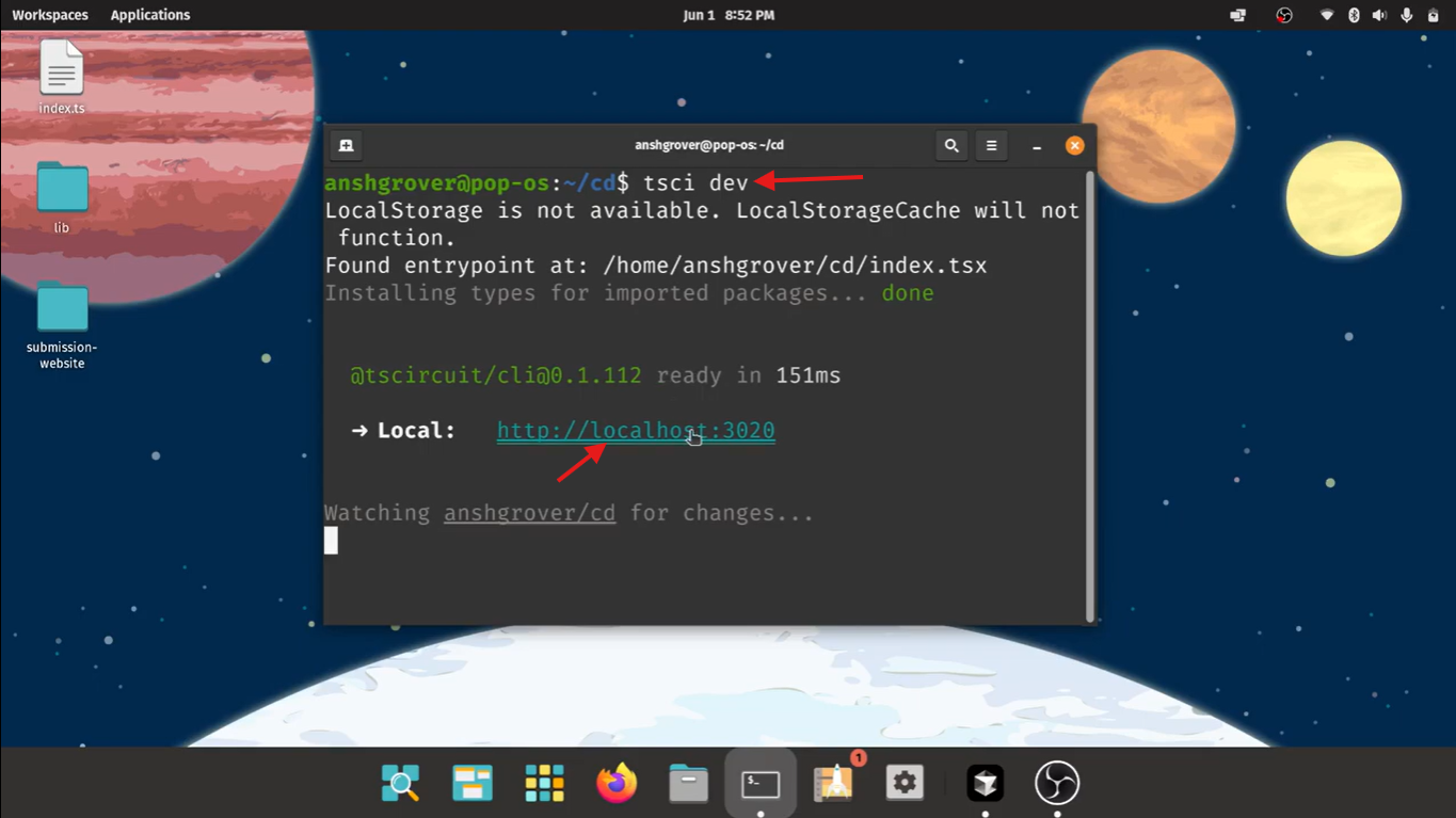 Run `tsci dev` to start the development server
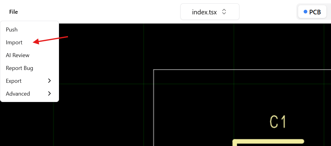 In the tsci dev environment, navigate to "File -> Import"
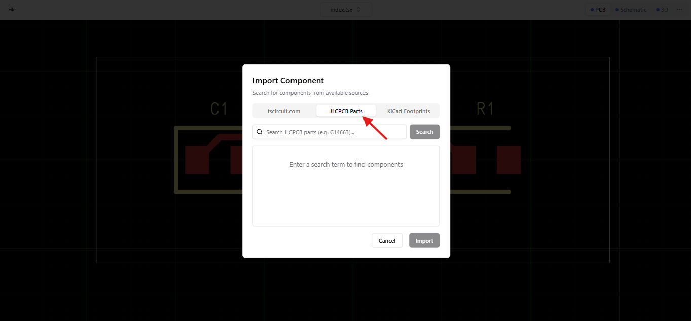 Go to the JLCPCB Parts tab and search by part number (e.g., 'C5100227') or keyword (e.g., 'ESP32')
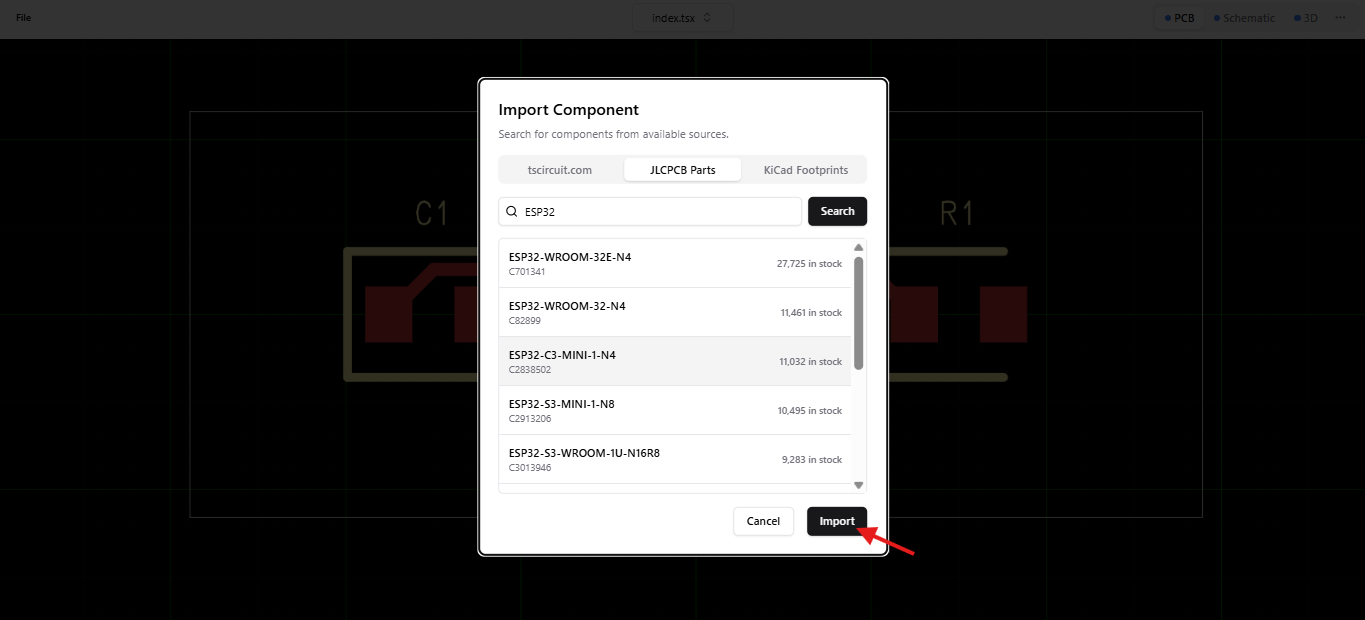 Select component and click Import
After importing, you can use the component in your circuit like this:
### Example Usage
```tsx
import { ComponentName } from "@tsci/imported-component"
export default () => (
)
```
:::tip Tip
Using File > Import from the editor locally is recommended
:::
## Import Using Web UI
You can import JLCPCB components on [tscircuit.com](https://tscircuit.com). After
importing the snippet, it'll be given a package name like `@tsci/YOUR_NAME.CHIP_NAME`
and available for import from the tscircuit registry.
Select component and click Import
After importing, you can use the component in your circuit like this:
### Example Usage
```tsx
import { ComponentName } from "@tsci/imported-component"
export default () => (
)
```
:::tip Tip
Using File > Import from the editor locally is recommended
:::
## Import Using Web UI
You can import JLCPCB components on [tscircuit.com](https://tscircuit.com). After
importing the snippet, it'll be given a package name like `@tsci/YOUR_NAME.CHIP_NAME`
and available for import from the tscircuit registry.
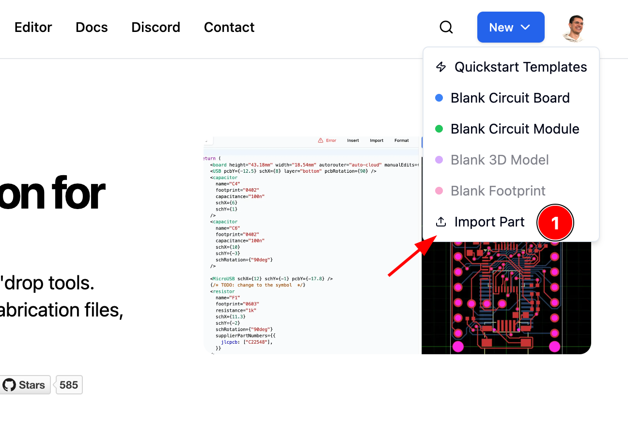 Step 1: Go to `tscircuit.com` and press the "new" button
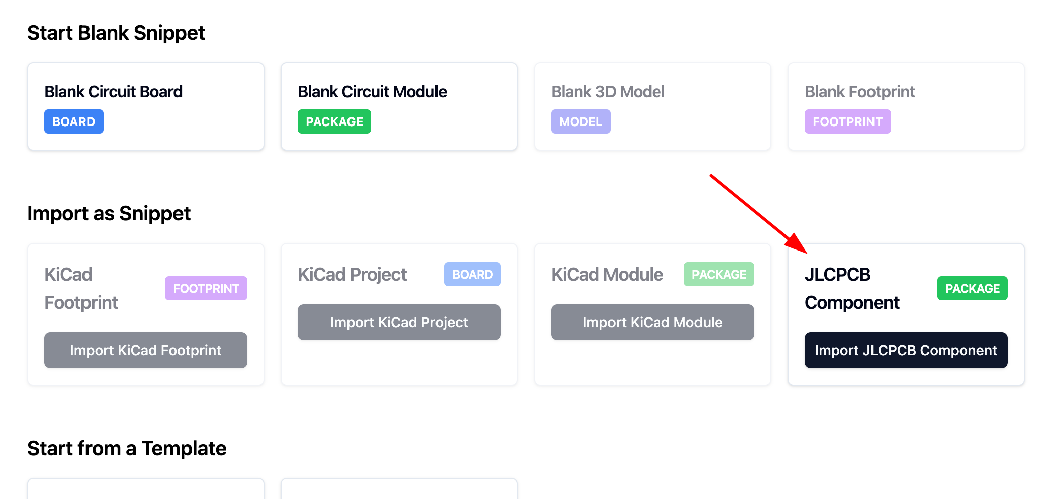 Step 2: Click "Import JLCPCB Component"
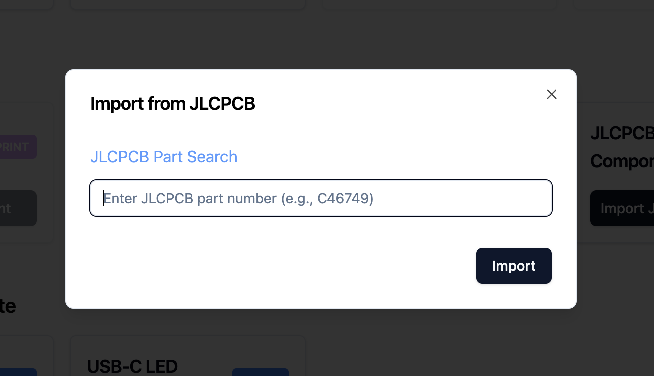 Step 3: Paste in the JLCPCB Part Number
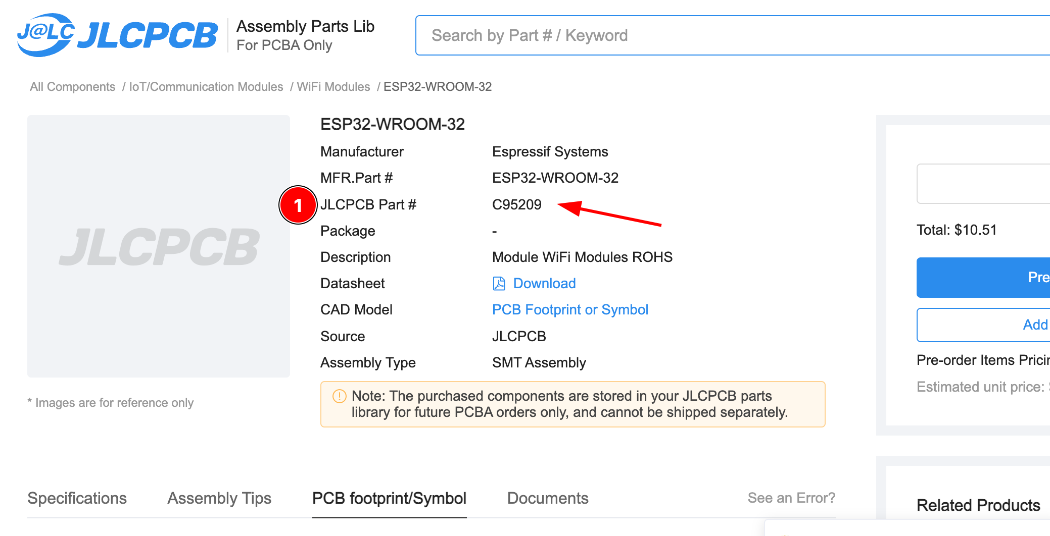 You can find the JLCPCB Part Number on JLCPCB's website
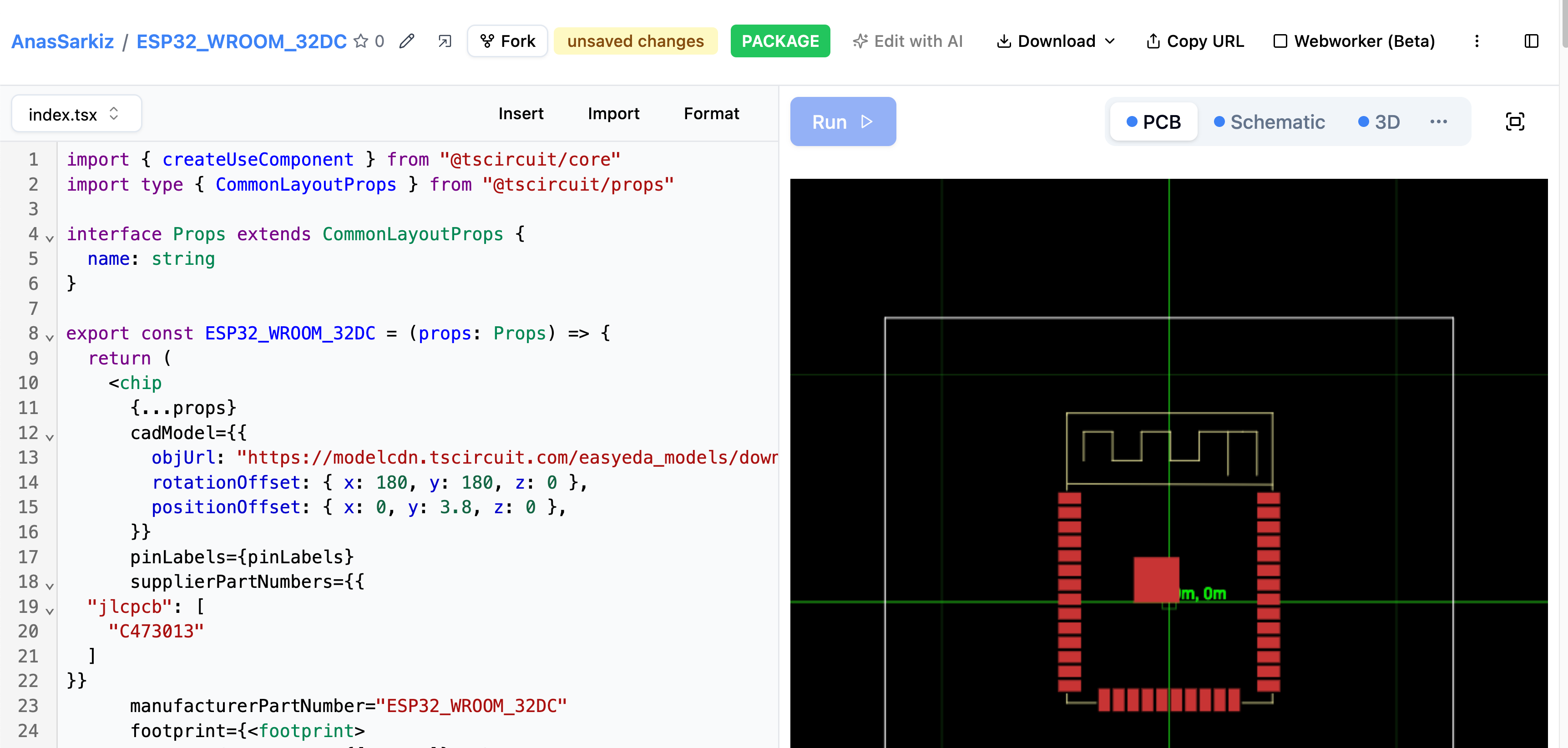 An example of an imported JLCPCB component
After your component has been added to tscircuit, you can import it as a
`@tsci/*` import like this:
```tsx
import { ESP32_WROOM_32DC } from "@tsci/AnasSarkiz.ESP32_WROOM_32DC"
export default () => (
)
```
---
title: Importing from KiCad
sidebar_position: 3
description: You can import KiCad components or projects into tscircuit.
---
## Overview
You can import KiCad components or projects into tscircuit.
:::tip
If you're trying to use a footprint from KiCad's standard libraries, you can skip manual importing and reference it directly with the `kicad:` prefix (e.g. `kicad:Resistor_SMD/R_0402_1005Metric`). See [KiCad Footprints](/footprints/kicad-footprints) for more details.
:::
To import from KiCad, you should understand the different file formats KiCad
uses:
- Files for KiCad components
- `kicad_mod` - PCB footprint file for a single component
- `kicad_sym` - Schematic symbol file for a single component
- Files for KiCad projects
- `kicad_pro` - KiCad project file
- `kicad_pcb` - KiCad PCB board file
- `kicad_sch` - KiCad Schematic board file
:::info
We're still building KiCad import directly into tscircuit.com, stay tuned for
when that's available!
:::
## Importing KiCad Components
Currently the easiest way to import KiCad components is to go to [kicad-component.tscircuit.com](https://kicad-component.tscircuit.com/)
and upload your `kicad_mod` and/or `kicad_sym` file.
### Importing KiCad Components using the CLI
Using tscircuit's [open-source KiCad component converter](https://github.com/tscircuit/kicad-component-converter),
we can convert KiCad files on the command line.
First install the component converter:
```bash
npm install -g kicad-component-converter
```
Next, run the following command to convert your KiCad files:
```bash
# Convert a directory ./my-footprints.pretty to a tscircuit project
kicad-component-converter convert-kicad-directory --input-dir ./my-footprints.pretty --output-dir ./my-tscircuit-footprints
```
### Importing `.kicad_pcb` files directly
You can import a KiCad PCB board file as Circuit JSON and place it inside a
tscircuit board with ``:
```tsx
import { circuitJson } from "./example.kicad_pcb"
circuit.add(
,
)
```
### Importing KiCad Components Programmatically
```bash
bun add kicad-component-converter
```
#### Import `.kicad_mod` files directly
`kicad-component-converter` registers a bundler loader that lets you import KiCad
footprints like any other module inside your tscircuit project:
```tsx
import kicadMod from "./footprint.kicad_mod"
export default () => {
return (
)
}
```
#### Convert KiCad files manually
If you need to do the conversion yourself (for example inside a build script),
you can read the `.kicad_mod` file and pass it through the parser:
```tsx
import { parseKicadModToCircuitJson } from "kicad-component-converter"
import { readFileSync } from "node:fs"
const fileContent = readFileSync("SW_SP3T_PCM13.kicad_mod")
const circuitJson = await parseKicadModToCircuitJson(fileContent)
/* [
* {
* "type": "pcb_smtpad",
* "x": 0.345,
* ...
*/
```
[Circuit JSON](https://github.com/tscircuit/circuit-json) can then be converted
into regular tscircuit modules using [circuit-json-to-tscircuit](https://github.com/tscircuit/circuit-json-to-tscircuit)
---
title: Installing KiCad Libraries
sidebar_position: 4
description: Install KiCad footprint libraries from GitHub and use them in your tscircuit projects with full TypeScript support.
---
## Overview
You can install KiCad footprint libraries directly from GitHub using the `tsci add` or `tsci install` command. This is the easiest way to use existing KiCad footprints in your tscircuit projects, with automatic TypeScript type generation for full IDE support.
## Installation
To install a KiCad library from GitHub, use the `tsci add` command with the repository URL:
```bash
tsci add https://github.com/espressif/kicad-libraries
```
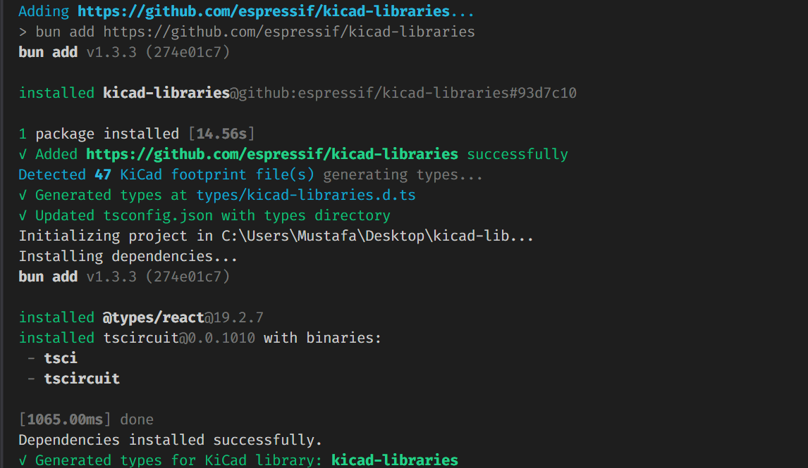
:::tip
`tsci install` is an alias for `tsci add` - both commands work identically.
:::
## What Happens During Installation
When you install a repository containing `.kicad_mod` files, `tsci` will automatically:
1. **Add the package to `package.json`** - The library is added as a dependency
2. **Install in `node_modules`** - The package is downloaded and installed
3. **Detect KiCad footprints** - Scans for `.kicad_mod` files in the repository
4. **Generate TypeScript types** - Creates type definitions in `types/.d.ts`
5. **Configure `tsconfig.json`** - Adds the types directory to `typeRoots`
## Using KiCad Footprints in Your Circuit
After installation, you can import `.kicad_mod` files directly in your circuit code:
```tsx
import kicadMod from "kicad-libraries/footprints/Espressif.pretty/ESP32-S2-MINI-1.kicad_mod"
export default () => {
return (
)
}
```
The imported `kicadMod` can be used directly as the `footprint` prop on components like ``.
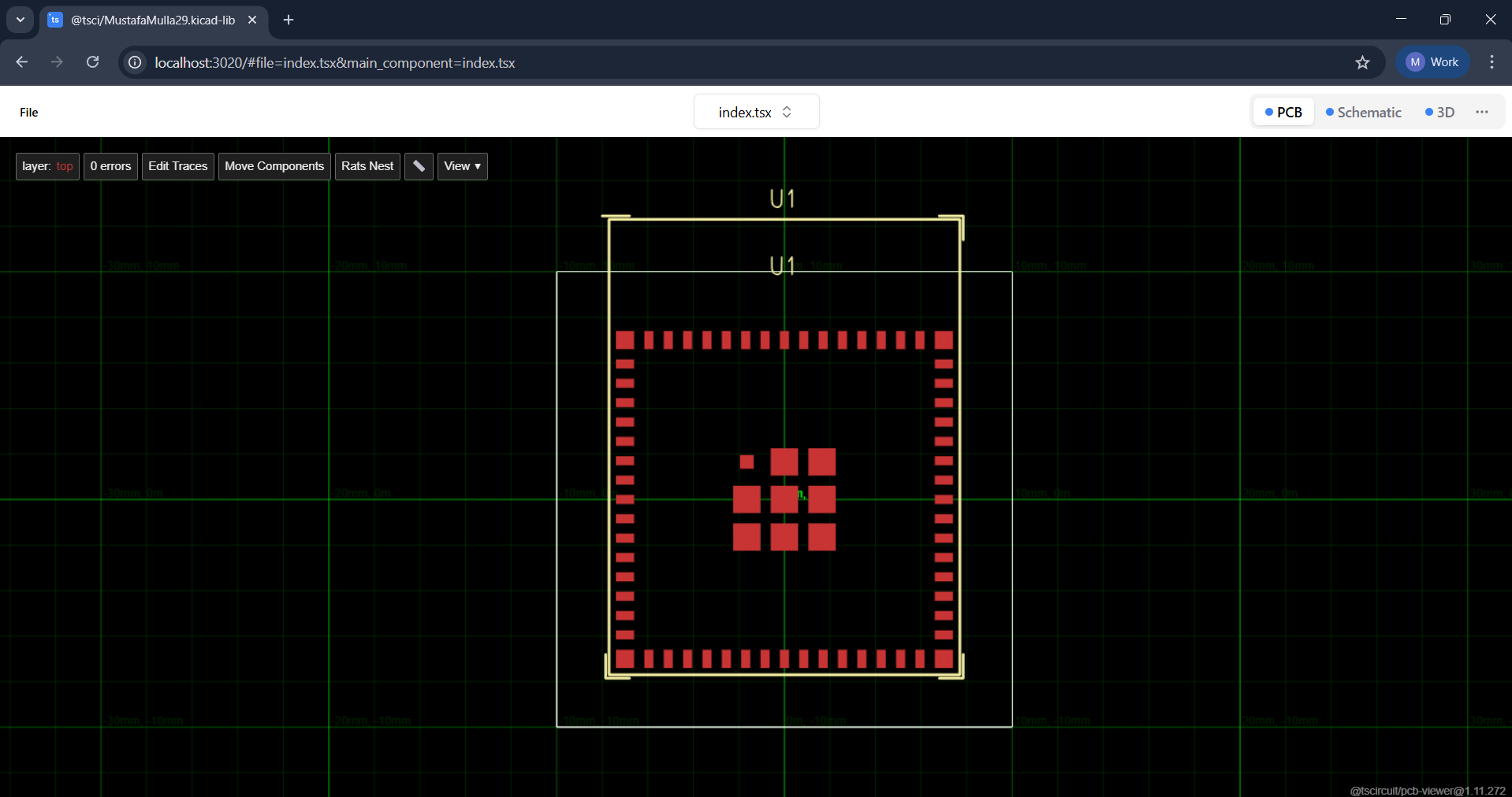
## Generated Type Definitions
When you install a KiCad library, `tsci` creates a type definition file in the `types/` directory. For example, installing `kicad-libraries` creates `types/kicad-libraries.d.ts`:
```typescript
declare module "kicad-libraries/footprints/Espressif.pretty/ESP32-S2-MINI-1.kicad_mod" {
const value: string
export default value
}
declare module "kicad-libraries/footprints/Espressif.pretty/ESP32-C3-MINI-1.kicad_mod" {
const value: string
export default value
}
// ... declarations for all .kicad_mod files in the library
```
This provides:
- **Full TypeScript support** - No type errors when importing `.kicad_mod` files
- **IDE autocomplete** - Your editor can suggest available footprint paths
- **Import validation** - Catch typos in import paths at compile time
## tsconfig.json Configuration
The command automatically updates your `tsconfig.json` to include the types directory:
```json
{
"compilerOptions": {
"typeRoots": ["./types", "./node_modules/@types"]
}
}
```
If your project doesn't have a `tsconfig.json`, one will be created with the necessary configuration.
## See Also
- [Importing from KiCad](/guides/importing-modules-and-chips/importing-from-kicad) - Other methods to import KiCad components
- [KiCad Footprints](/footprints/kicad-footprints) - Using KiCad's standard library footprints with the `kicad:` prefix
- [tsci add](/command-line/tsci-add) - Installing tscircuit registry packages
---
title: Exporting a KiCad Library
description: >-
Export your tscircuit designs as a KiCad library containing symbols,
footprints, and 3D models that can be reused across multiple KiCad projects.
---
## Overview
tscircuit allows you to export your circuit designs as a **KiCad Library**. Unlike the KiCad Project export (which creates a complete project file), the KiCad Library export creates reusable components that can be imported into any KiCad project.
The exported library includes:
- **Symbol Libraries** (`symbols/` folder) - Schematic symbols for all components
- **Footprint Libraries** (`footprints/` folder) - PCB footprints for all components
- **3D Models** (`3dmodels/` folder) - 3D model files (STEP/WRL) referenced by footprints
- **Library Tables** (`fp-lib-table`, `sym-lib-table`) - Configuration files for KiCad
## User vs Builtin Components
tscircuit automatically separates your components into two library categories:
### User Components
Components that use **custom footprints or symbols** are placed in the user library, named after your project (e.g., `my-library`). These include:
- Components with a custom `footprint` prop (JSX footprint definition):
```tsx
}
/>
```
- Components with a custom `symbol` prop (JSX symbol definition):
```tsx
}
/>
```
### Builtin Components
Components that use **standard footprinter strings** (e.g., `0402`, `soic8`) are placed in the `tscircuit_builtin` library. This includes all footprints that tscircuit supports by default.
## Directory Structure
```
my-library/
├── symbols/
│ ├── my-library.kicad_sym # User symbols (custom symbols)
│ └── tscircuit_builtin.kicad_sym # Builtin symbols (standard symbols)
├── footprints/
│ ├── my-library.pretty/ # User footprints
│ │ └── MyCustomSwitch.kicad_mod
│ └── tscircuit_builtin.pretty/ # Builtin footprints
│ ├── resistor_0402.kicad_mod
│ └── chip_soic8.kicad_mod
├── 3dmodels/
│ └── switch.step
├── fp-lib-table
└── sym-lib-table
```
## How to Export
### Using the Browser
1. Run `tsci dev` in your project directory
2. Navigate to **File > Export > KiCad Library**
3. A zip file will be downloaded containing all library files
### Using the CLI
```bash
tsci export ./lib/my-library.ts -f kicad-library
```
The CLI will:
1. Discover all component exports from the entry file
2. Build each component to circuit JSON
3. Extract and classify footprints/symbols (user vs builtin)
4. Generate the KiCad library files
## Using the Library in KiCad
1. **Extract/Copy the library** to your KiCad project folder or a shared libraries location
2. **Add the library tables** to your KiCad project:
- Copy `fp-lib-table` and `sym-lib-table` to your project folder, OR
- Merge the entries into your existing library tables
3. **Use the symbols and footprints** in your schematic and PCB:
- Custom symbols appear under your library name (e.g., `my-library`)
- Standard symbols appear under `tscircuit_builtin`
## Including 3D Models
Add a `cadModel` prop to include 3D models in your export:
```tsx
import stepUrl from "./switch.step"
}
/>
```
The 3D model will be:
- Referenced in the footprint file with the correct path
- Included in the `3dmodels/` folder of the export
---
title: KiCad Metadata
sidebar_position: 1
description: Document KiCad-specific metadata for footprints and symbols on tscircuit components
---
# KiCad Metadata
tscircuit components support KiCad-specific metadata properties that preserve information from KiCad footprint and symbol files. These properties are available on all normal components (chip, resistor, capacitor, etc.) and are useful when importing from KiCad or when you need to include KiCad-specific information in your exported designs.
## Properties Overview
| Property | Element | Description |
|----------|---------|-------------|
| `kicadFootprintMetadata` | Components | Metadata from KiCad footprint (`.kicad_mod`) files |
| `kicadSymbolMetadata` | Components | Metadata from KiCad symbol (`.kicad_sym`) files |
| `kicadPinMetadata` | `` | Metadata for KiCad pin electrical and visual properties |
---
## kicadFootprintMetadata
The `kicadFootprintMetadata` property stores metadata extracted from KiCad footprint files. This includes information about the footprint's properties, attributes, pads, and 3D model.
### Type Definition
```typescript
interface KicadFootprintMetadata {
footprintName?: string
version?: number | string
generator?: string
generatorVersion?: number | string
layer?: string
properties?: KicadFootprintProperties
attributes?: KicadFootprintAttributes
pads?: KicadFootprintPad[]
embeddedFonts?: boolean
model?: KicadFootprintModel
}
```
### Properties
#### Top-level Properties
| Property | Type | Description |
|----------|------|-------------|
| `footprintName` | `string` | Name identifier for the footprint |
| `version` | `number \| string` | KiCad file format version |
| `generator` | `string` | Tool that generated the footprint |
| `generatorVersion` | `number \| string` | Version of the generator tool |
| `layer` | `string` | Default layer (e.g., `"F.Cu"`) |
| `embeddedFonts` | `boolean` | Whether fonts are embedded in the footprint |
#### properties
Standard KiCad footprint properties for documentation:
```typescript
interface KicadFootprintProperties {
Reference?: KicadProperty // Component reference designator (e.g., "R1")
Value?: KicadProperty // Component value (e.g., "10k")
Datasheet?: KicadProperty // Link to component datasheet
Description?: KicadProperty // Human-readable description
}
interface KicadProperty {
value: string
at?: { x: number | string; y: number | string; rotation?: number | string }
layer?: string
uuid?: string
hide?: boolean
effects?: {
font?: {
size?: { x: number | string; y: number | string }
thickness?: number | string
}
}
}
```
#### attributes
Footprint manufacturing attributes:
```typescript
interface KicadFootprintAttributes {
through_hole?: boolean // THT component
smd?: boolean // SMD component
exclude_from_pos_files?: boolean // Exclude from pick-and-place
exclude_from_bom?: boolean // Exclude from bill of materials
}
```
#### pads
Array of pad definitions:
```typescript
interface KicadFootprintPad {
name: string // Pad name/number
type: string // Pad type (e.g., "smd", "thru_hole")
shape?: string // Pad shape (e.g., "rect", "circle", "oval")
at?: { x: number | string; y: number | string; rotation?: number | string }
size?: { x: number | string; y: number | string }
drill?: number | string // Drill diameter for THT pads
layers?: string[] // Copper layers (e.g., ["F.Cu", "F.Paste"])
removeUnusedLayers?: boolean
uuid?: string
}
```
#### model
3D model reference and transforms:
```typescript
interface KicadFootprintModel {
path: string // Path to 3D model file
offset?: { x: number | string; y: number | string; z: number | string }
scale?: { x: number | string; y: number | string; z: number | string }
rotate?: { x: number | string; y: number | string; z: number | string }
}
```
### Example Usage
```tsx
```
---
## kicadSymbolMetadata
The `kicadSymbolMetadata` property stores metadata extracted from KiCad symbol files. This includes schematic-specific information like pin configuration, BOM settings, and symbol properties.
### Type Definition
```typescript
interface KicadSymbolMetadata {
symbolName?: string
extends?: string
pinNumbers?: KicadSymbolPinNumbers
pinNames?: KicadSymbolPinNames
excludeFromSim?: boolean
inBom?: boolean
onBoard?: boolean
properties?: KicadSymbolProperties
embeddedFonts?: boolean
}
```
### Properties
#### Top-level Properties
| Property | Type | Description |
|----------|------|-------------|
| `symbolName` | `string` | Symbol identifier name |
| `extends` | `string` | Parent symbol for inheritance |
| `excludeFromSim` | `boolean` | Exclude from SPICE simulation |
| `inBom` | `boolean` | Include in bill of materials |
| `onBoard` | `boolean` | Component appears on PCB |
| `embeddedFonts` | `boolean` | Whether fonts are embedded |
#### pinNumbers
Pin number display configuration:
```typescript
interface KicadSymbolPinNumbers {
hide?: boolean // Hide pin numbers in schematic
}
```
#### pinNames
Pin name display configuration:
```typescript
interface KicadSymbolPinNames {
offset?: number | string // Distance from pin to name text
hide?: boolean // Hide pin names in schematic
}
```
#### properties
Standard KiCad symbol properties:
```typescript
interface KicadSymbolProperties {
Reference?: KicadSymbolProperty // Reference designator prefix (e.g., "U")
Value?: KicadSymbolProperty // Component value/name
Footprint?: KicadSymbolProperty // Associated footprint
Datasheet?: KicadSymbolProperty // Datasheet URL
Description?: KicadSymbolProperty // Human-readable description
ki_keywords?: KicadSymbolProperty // Search keywords
ki_fp_filters?: KicadSymbolProperty // Footprint filter patterns
}
interface KicadSymbolProperty {
value: string
id?: number | string
at?: { x: number | string; y: number | string; rotation?: number | string }
effects?: {
font?: {
size?: { x: number | string; y: number | string }
thickness?: number | string
}
justify?: string | string[]
hide?: boolean
}
}
```
### Example Usage
```tsx
```
---
## kicadPinMetadata
The `kicadPinMetadata` property is used on `` elements to store KiCad-specific pin information. This includes the pin's electrical type, graphic style, and text sizing properties that are used when exporting to KiCad symbol files.
### Type Definition
```typescript
interface KicadPinMetadata {
electricalType?: KicadPinElectricalType
graphicStyle?: KicadPinGraphicStyle
pinLength?: Distance
nameTextSize?: Distance
numberTextSize?: Distance
}
```
### Properties
| Property | Type | Description |
|----------|------|-------------|
| `electricalType` | `KicadPinElectricalType` | Electrical characteristics of the pin |
| `graphicStyle` | `KicadPinGraphicStyle` | Visual representation style of the pin |
| `pinLength` | `Distance` | Physical length of the pin |
| `nameTextSize` | `Distance` | Text size for the pin name label |
| `numberTextSize` | `Distance` | Text size for the pin number label |
#### electricalType
Specifies the electrical characteristics of the pin:
| Value | Description |
|-------|-------------|
| `"input"` | Input pin |
| `"output"` | Output pin |
| `"bidirectional"` | Bidirectional pin |
| `"tri_state"` | Tri-state pin |
| `"passive"` | Passive pin (resistors, capacitors, etc.) |
| `"free"` | Free pin (can connect to anything) |
| `"unspecified"` | Unspecified electrical type |
| `"power_in"` | Power input pin (VCC, GND) |
| `"power_out"` | Power output pin |
| `"open_collector"` | Open collector output |
| `"open_emitter"` | Open emitter output |
| `"no_connect"` | No connection pin |
#### graphicStyle
Defines the visual representation of the pin in schematics:
| Value | Description |
|-------|-------------|
| `"line"` | Simple line (default) |
| `"inverted"` | Inverted (bubble) |
| `"clock"` | Clock input indicator |
| `"inverted_clock"` | Inverted clock |
| `"input_low"` | Active low input |
| `"clock_low"` | Active low clock |
| `"output_low"` | Active low output |
| `"falling_edge_clock"` | Falling edge triggered clock |
| `"nonlogic"` | Non-logic pin |
### Example Usage
```tsx
```
---
## When to Use KiCad Metadata
### Importing from KiCad
When you [import components from KiCad](/guides/importing-modules-and-chips/importing-from-kicad), the converter tools automatically populate these metadata properties. This preserves the original KiCad information for reference and export compatibility.
### Exporting to KiCad
When exporting your tscircuit design to KiCad format, these metadata properties are used to generate accurate `.kicad_mod` and `.kicad_sym` files that maintain compatibility with KiCad workflows.
## Related Documentation
- [Importing from KiCad](/guides/importing-modules-and-chips/importing-from-kicad) - How to import KiCad components
- [KiCad Footprints](/footprints/kicad-footprints) - Using KiCad footprints with the `kicad:` prefix
- [Installing KiCad Libraries](/guides/importing-modules-and-chips/installing-kicad-libraries-from-github) - Adding KiCad libraries to your project
---
title: Using tscircuit KiCad PCM URLs
description: >-
Install tscircuit component libraries directly into KiCad using the Plugin and
Content Manager (PCM) with cloud-hosted repository URLs.
---
## Overview
tscircuit packages can be installed directly into KiCad using the **Plugin and Content Manager (PCM)**. Each published tscircuit package includes a KiCad PCM URL that points to a repository hosted on `tscircuit.app` containing the symbols, footprints, and 3D models for all components in the package.
This guide walks you through the process of adding a tscircuit package to KiCad using the PCM URL.
## Step 1: Find the KiCad PCM URL
Navigate to your tscircuit package page on [tscircuit.com](https://tscircuit.com). In the **Releases** section on the right sidebar, you'll find a **KiCad PCM URL** link. If you don't see this link, enable `kicadPcm` in your tscircuit config (see [tscircuit config](https://docs.tscircuit.com/guides/tscircuit-essentials/tscircuit-config)).
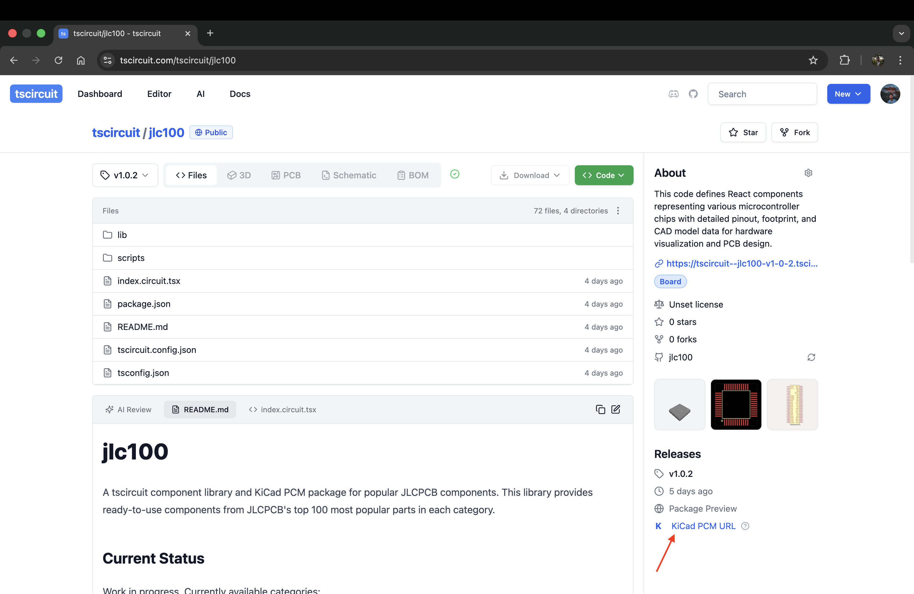
## Step 2: Copy the Repository URL
Click the **KiCad PCM URL** link to open the repository JSON file in your browser. Copy the full URL from the address bar.
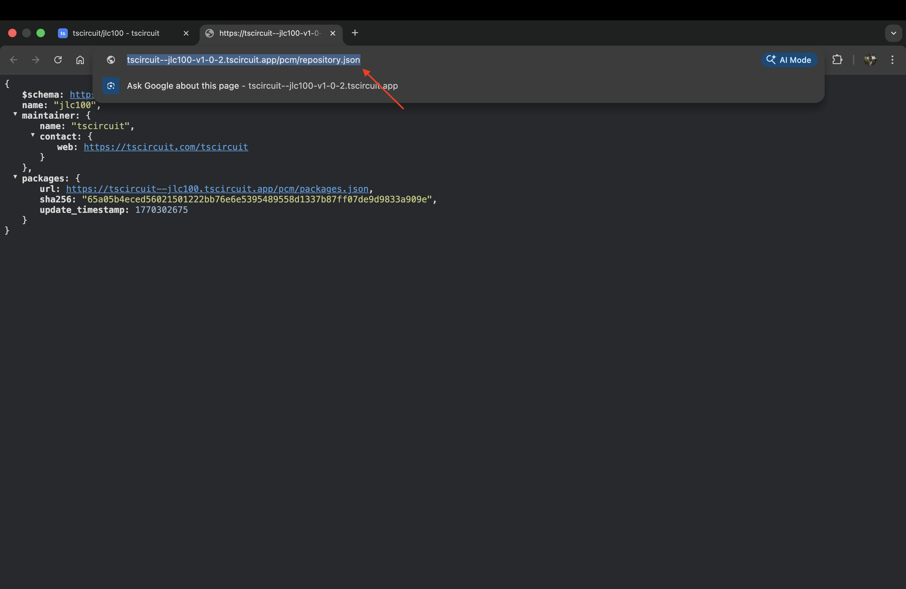
## Step 3: Add the Repository in KiCad PCM
1. Open KiCad and go to **Tools > Plugin and Content Manager**
2. Click the **Manage...** button in the top-right corner
3. In the "Manage Repositories" dialog, click the **+** button to add a new repository
4. Paste the repository URL you copied and click **OK**
5. Click **Save** to save the repository configuration
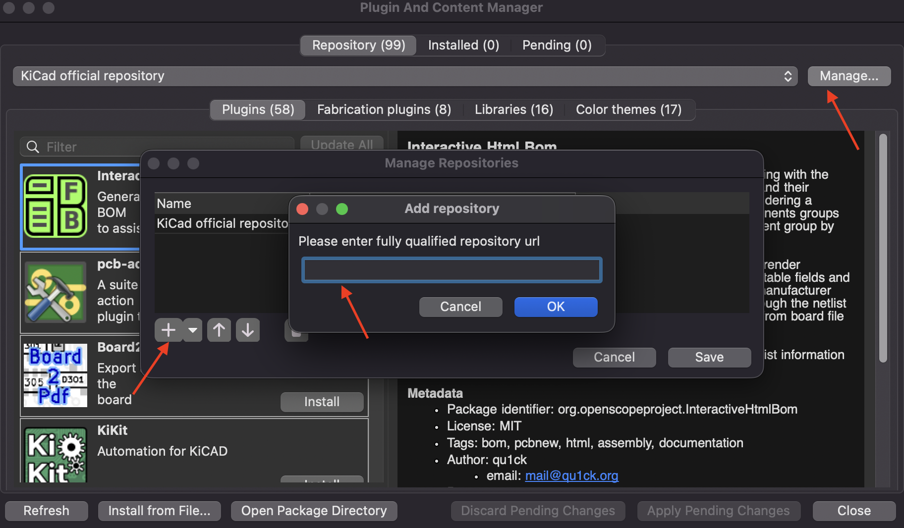
## Step 4: Select the Repository
After saving, use the repository dropdown at the top-left of the PCM window to select your newly added tscircuit repository.
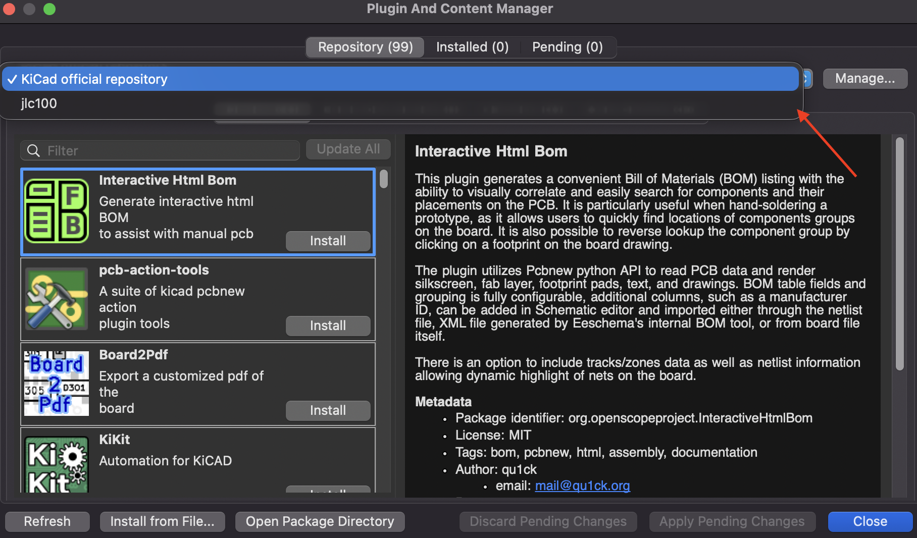
## Step 5: Install the Library
1. Navigate to the **Libraries** tab
2. Select the tscircuit library package from the list
3. Click the **Install** button
4. Click **Apply Pending Changes** at the bottom of the window to begin the installation
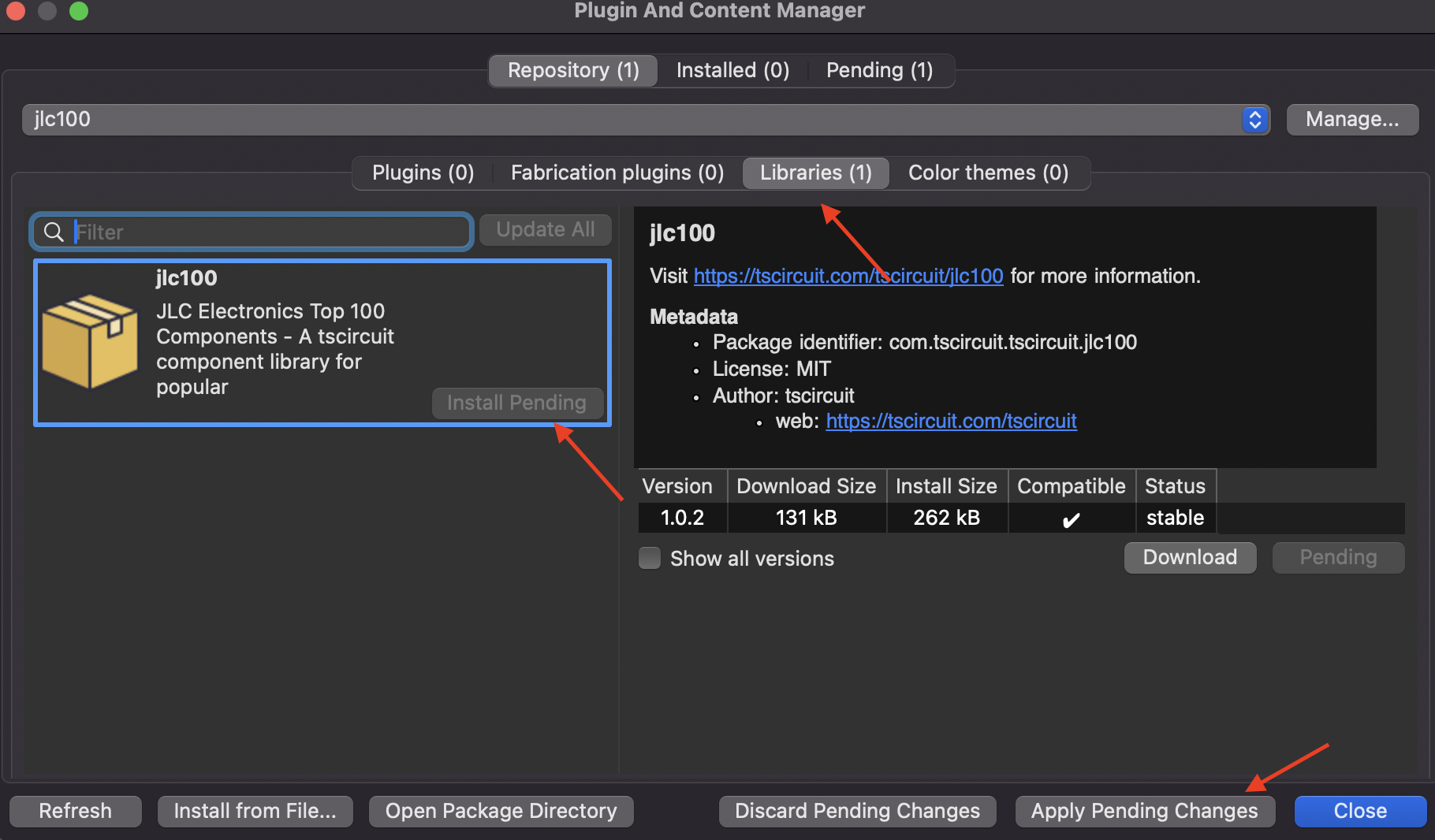
The download progress will be displayed:
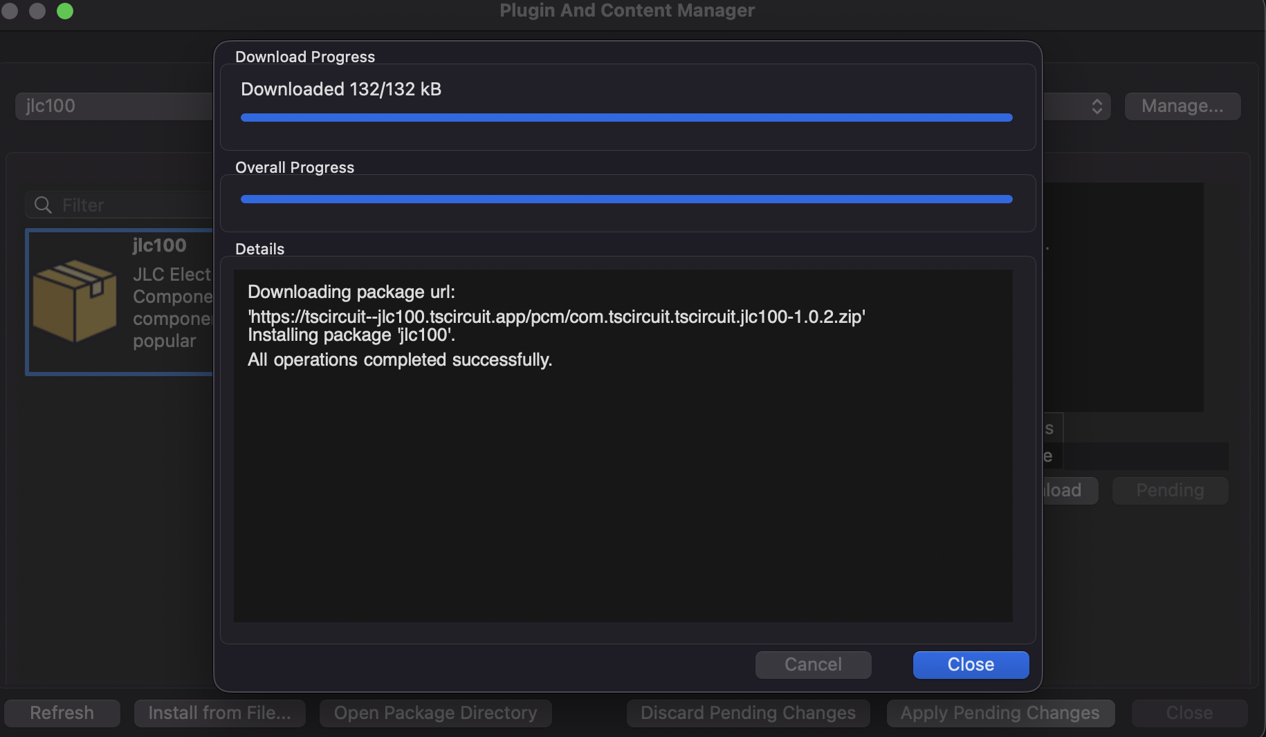
## Step 6: Verify Installation
Once the installation is complete, switch to the **Installed** tab to verify that the library appears in your installed packages list.
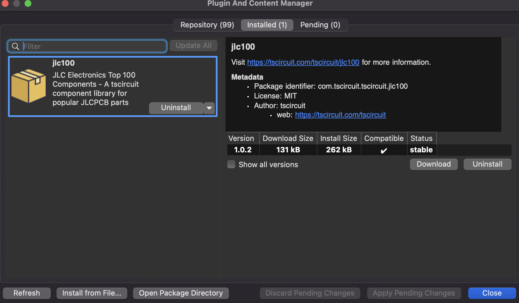
## Step 7: Use the Library in Your Project
The library is now ready to use in your KiCad projects. Open the **Schematic Editor** and use **Add Symbol** (shortcut: `A`) to browse and place components from the installed library.
The components will appear under a library name prefixed with `PCM_` (e.g., `PCM_jlc100`).
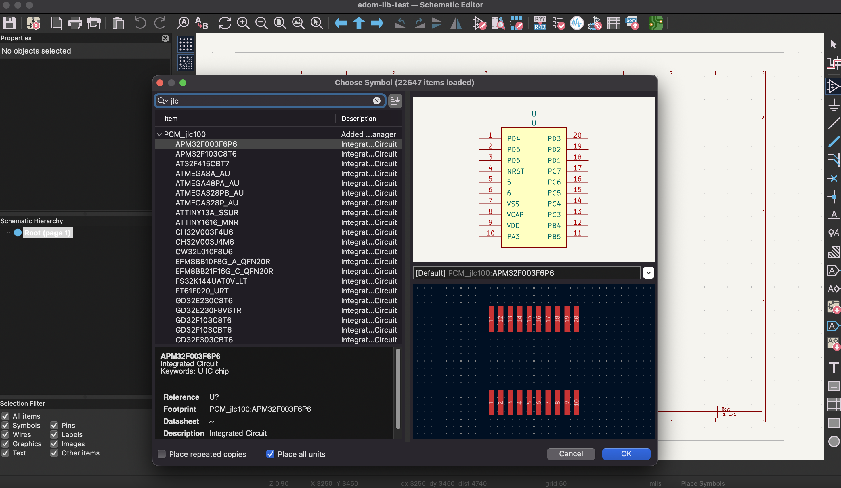
---
title: Measuring circuit size using scripts
description: Use @tscircuit/core to evaluate groups, extract bounding boxes, and pick board templates that fit
---
Automating board design often starts with a question: _how much space does this group of parts actually need?_ This guide shows how to render groups inside a script, capture their dimensions, and store metadata that other steps in your pipeline can read.
## Recommended workflow
1. Keep each reusable group in a `design-groups/` directory so it can be evaluated on its own.
2. Run a script that loads every group, renders it with `tscircuit`, and saves a metadata JSON file containing width and height.
3. When you build the final board component, import the metadata file to decide which carrier template has enough room.
Separating generated metadata from hand-authored TSX keeps the process debuggable. If you _do_ write metadata back into a `.tsx` file, wrap the generated block in clearly marked comments so humans and tools know where automation can safely write.
## Directory layout
```text
my-project/
├─ design-groups/
│ ├─ esp32-breakout.tsx # Exports the group you want to analyze
│ └─ esp32-breakout.metadata.json # Width/height baked by the script
├─ carriers/
│ └─ esp32-breakout-carrier.tsx # Imports metadata when building the final board
└─ scripts/
└─ bake-group-metadata.ts # Script that renders the group and writes JSON
```
Each group file should export a React component that renders a `` inside a `` or within the structure you normally use. The script can then import it, render it in isolation, and evaluate the results.
```tsx title="design-groups/esp32-breakout.tsx"
export const Esp32Breakout = () => (
{/* Components, nets, and layout props */}
)
```
## Rendering a group and measuring its bounding box
The snippet below renders a group, waits for placement to settle, and then extracts the PCB group bounds from Circuit JSON.
```tsx
import { RootCircuit } from "tscircuit"
import { Esp32Breakout } from "../design-groups/esp32-breakout"
const circuit = new RootCircuit()
circuit.add(
)
await circuit.renderUntilSettled();
const circuitJson = await circuit.getCircuitJson();
const rootGroupOrBoard = circuitJson.find(
(item) =>
item.type === "pcb_board" ||
(item.type === "pcb_group" && item.is_subcircuit),
);
Bun.write("../design-groups/esp32-breakout.metadata.json", JSON.stringify(rootGroupOrBoard, null, 2));
```
You can do this dynamically for every file in the `design-groups` directory:
```tsx
import { RootCircuit } from "tscircuit"
for (const file of await Bun.glob("design-groups/*.tsx")) {
const { default: GroupComponent } = await import(`../${file}`);
const groupName = file.split("/").pop()?.replace(".tsx", "");
const circuit = new RootCircuit();
circuit.add();
await circuit.renderUntilSettled();
const circuitJson = await circuit.getCircuitJson();
const rootGroupOrBoard = circuitJson.find(
(item) =>
item.type === "pcb_board" ||
(item.type === "pcb_group" && item.is_subcircuit),
);
await Bun.write(
`../design-groups/${groupName}.metadata.json`,
JSON.stringify(rootGroupOrBoard, null, 2)
);
}
```
## Detecting packing failures programmatically
Packing issues (such as overlaps or components outside the board) are surfaced in Circuit JSON as elements whose `type` ends in `_error`, for example `pcb_placement_error`, `pcb_footprint_overlap_error`, and `pcb_component_outside_board_error`. You can scan for them before trusting the bounding box.
```ts
function getPackingErrors(json: CircuitJson) {
return json.filter(
(element) =>
element.type.startsWith("pcb_") && element.type.endsWith("_error"),
)
}
```
If `getPackingErrors` returns any elements, skip writing metadata and log the error messages so you can debug the group in isolation. You can also persist the raw JSON to disk for later inspection or feed it into tools like `circuitjson.com`.
## Trying candidate board sizes
Once you can render a group programmatically, you can try it against a list of candidate board footprints and pick the smallest one that succeeds. Render the group inside a `` that has the candidate size, check for packing errors, and return the first success.
```tsx
const CANDIDATE_SIZES = [
{ name: "SMALL", width: 21, height: 51 },
{ name: "MEDIUM", width: 24, height: 58 },
]
async function findSmallestBoard(load: () => Promise) {
for (const size of CANDIDATE_SIZES) {
const circuit = new RootCircuit()
const Circuit = await load()
circuit.add(
,
)
await circuit.renderUntilSettled()
const json = (await circuit.getCircuitJson()) as CircuitJson
if (getPackingErrors(json).length === 0) {
return { size, json }
}
}
throw new Error("No candidate board size could pack the circuit")
}
```
With this helper you can run multiple passes: one to bake metadata for inspection, and another to select the best board footprint automatically. Store the selected board ID alongside the size metadata so later steps (such as generating headers or enclosure geometry) can read the decision without re-running the analysis.
## Using the baked metadata in a board component
The final board component can import the JSON and pick a template accordingly. Because the metadata is static, you can safely load it during module evaluation.
```tsx
import metadata from "../design-groups/esp32-breakout.metadata.json" assert { type: "json" }
const TEMPLATE_OPTIONS = [
{ id: "SMALL", width: 21, height: 51 },
{ id: "MEDIUM", width: 24, height: 58 },
]
const selectedTemplate = TEMPLATE_OPTIONS.find(
(option) =>
option.width >= metadata.width && option.height >= metadata.height,
)
if (!selectedTemplate) {
throw new Error("No board template can fit the baked group bounds")
}
export const Esp32BreakoutCarrier = ({ children }: { children: React.ReactNode }) => (
{children}
)
```
When automation needs to update the layout (for example, after rerunning packing with AI assistance), rerun the baking script to regenerate the JSON and let the board component pick a new template automatically. This keeps generated numbers out of your hand-authored TSX while remaining easy to audit.
You can add a script inside your package.json file to run the baking script:
```json
{
"scripts": {
"bake-metadata": "bun run scripts/bake-metadata.ts"
}
}
```
---
title: Building a Static Site
description: "`tsci build --site` packages your tscircuit project into a static website that anyone can browse without running a server."
---
`tsci build --site` packages your tscircuit project into a static website that anyone can browse without running a server. The command evaluates your circuits, exports the generated assets into a `dist` folder, and wires them up to the tscircuit RunFrame viewer so visitors can flip between PCB, schematic, and 3D previews right in the browser.
The [Common tscircuit gallery](https://common.tscircuit.com/) is an example of a site generated with this workflow.
## Prerequisites
Before building a site, make sure you have:
- A tscircuit project with one or more `*.circuit.tsx` files or another supported entrypoint.
- The tscircuit CLI installed (`npm install -g tsci`, `bunx tsci`, or `npx tsci`).
- Any dependencies that your circuits import (registry components, local packages, etc.).
## Building the site
Run the build command from the root of your project:
```bash
# generates dist/index.html and other assets
npx tsci build --site
```
The CLI resolves your entrypoint, evaluates every circuit, and then writes a static site to `dist/site/` alongside the usual `dist/circuit.json` outputs. The generated folder contains:
- `index.html` – a ready-to-host viewer.
- `lib/…/circuit.json` – one JSON file per design so the viewer can lazy load each project.
- Supporting JavaScript, CSS, and WebAssembly bundles for the RunFrame UI.
You can inspect the result locally with any static file server, for example:
```bash
npx serve dist
```
Opening `http://localhost:3000` (or the port reported by your static server) shows the same interactive viewer experience used at common.tscircuit.com.
## Customizing the catalog
The site automatically lists every circuit that `tsci build` evaluates. If you already use a `tscircuit.config.json` file, the same settings shape the static catalog: `mainEntrypoint` lets you pick a custom starting file, and the existing include/exclude patterns limit which `*.circuit.tsx` sources are exported.
When you add extra documentation or screenshots, keep them in a public asset folder (for example `public/`), then point to them from your circuits. Static assets referenced at build time are copied into `dist` so they ship with the site bundle.
## Deploying to Vercel
Vercel can host the generated site without any special adapters:
1. Push your project to GitHub or GitLab.
2. Create a new Vercel project that points to the repository.
3. Set the **Build Command** to `npx tsci build --site` (or `bunx tsci build --site` if you prefer Bun).
4. Set the **Output Directory** to `dist`.
5. Trigger a deploy – Vercel runs the build, uploads the static folder, and serves it on your chosen domain.
For preview deployments, Vercel repeats these steps on every pull request so reviewers can browse the circuits before merging.
## Deploying elsewhere
Because the output is plain HTML/JS/CSS, you can host it almost anywhere:
- **GitHub Pages** – run `npx tsci build --site` in CI and publish the `dist` folder to `gh-pages`.
- **Netlify** – configure the build command and output directory just like Vercel.
- **S3/CloudFront or static buckets** – upload the generated files with `aws s3 sync dist s3://your-bucket`.
Once deployed, the site stays fast and inexpensive to serve because no server-side rendering or API proxy is required—the viewer fetches the prebuilt `circuit.json` files directly from storage.
---
title: Connect GitHub Repositories to tscircuit
description: Link your project repo to tscircuit for automatic previews and publishing
---
You can connect your GitHub repositories to tscircuit to automatically
publish updates, access instant previews and make sharing boards easier.
You'll want to use the [command line tool](../../intro/quickstart-cli.md) to initialize
an application and push to tscircuit.com using [`tsci push`](../../command-line/tsci-push.md)
After that, navigate to the tscircuit.com page for your circuit and click "Connect to GitHub"
button on the right side of the page.
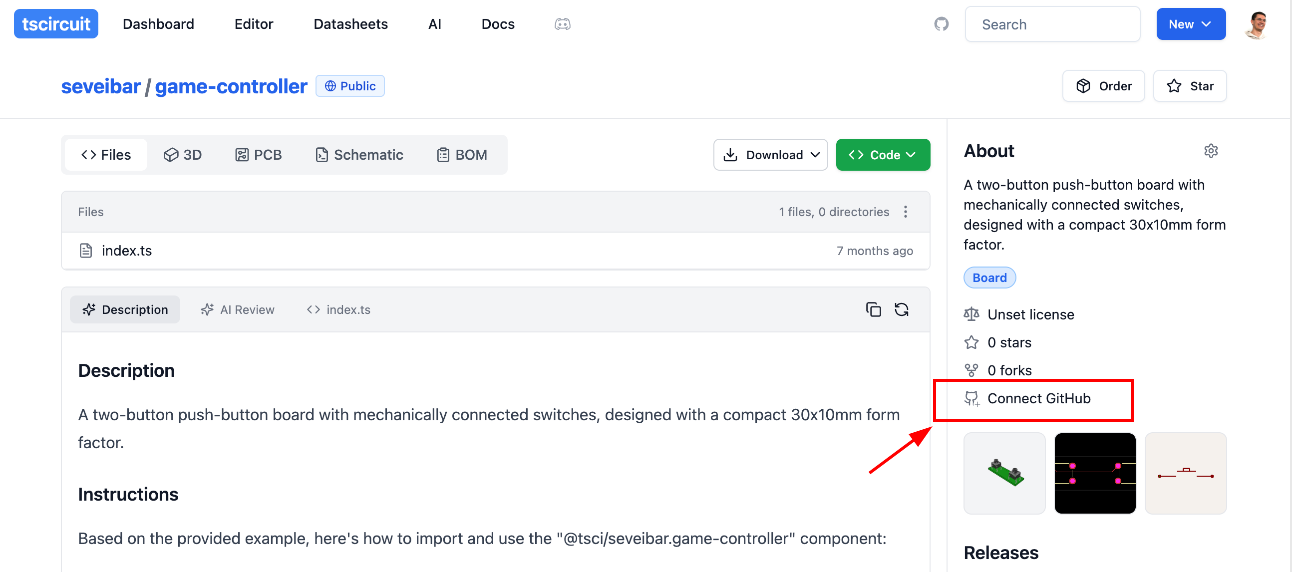
After connecting to GitHub, every time you merge a small GitHub action will
run to update the circuit on tscircuit.com. You
---
title: Displaying Circuit JSON on a Webpage
description: Render Circuit JSON in web apps using RunFrame and related components
---
[Circuit JSON](https://github.com/tscircuit/circuit-json) is a universal
intermediary format for representing an electronic circuit. It contains PCB,
Schematic, 3D, Bill of Materials and simulation information.
tscircuit code always converts into Circuit JSON, which can be displayed in
any of our React components
:::tip
You can also upload your Circuit JSON to [circuitjson.com](https://circuitjson.com)
for a quick preview!
:::
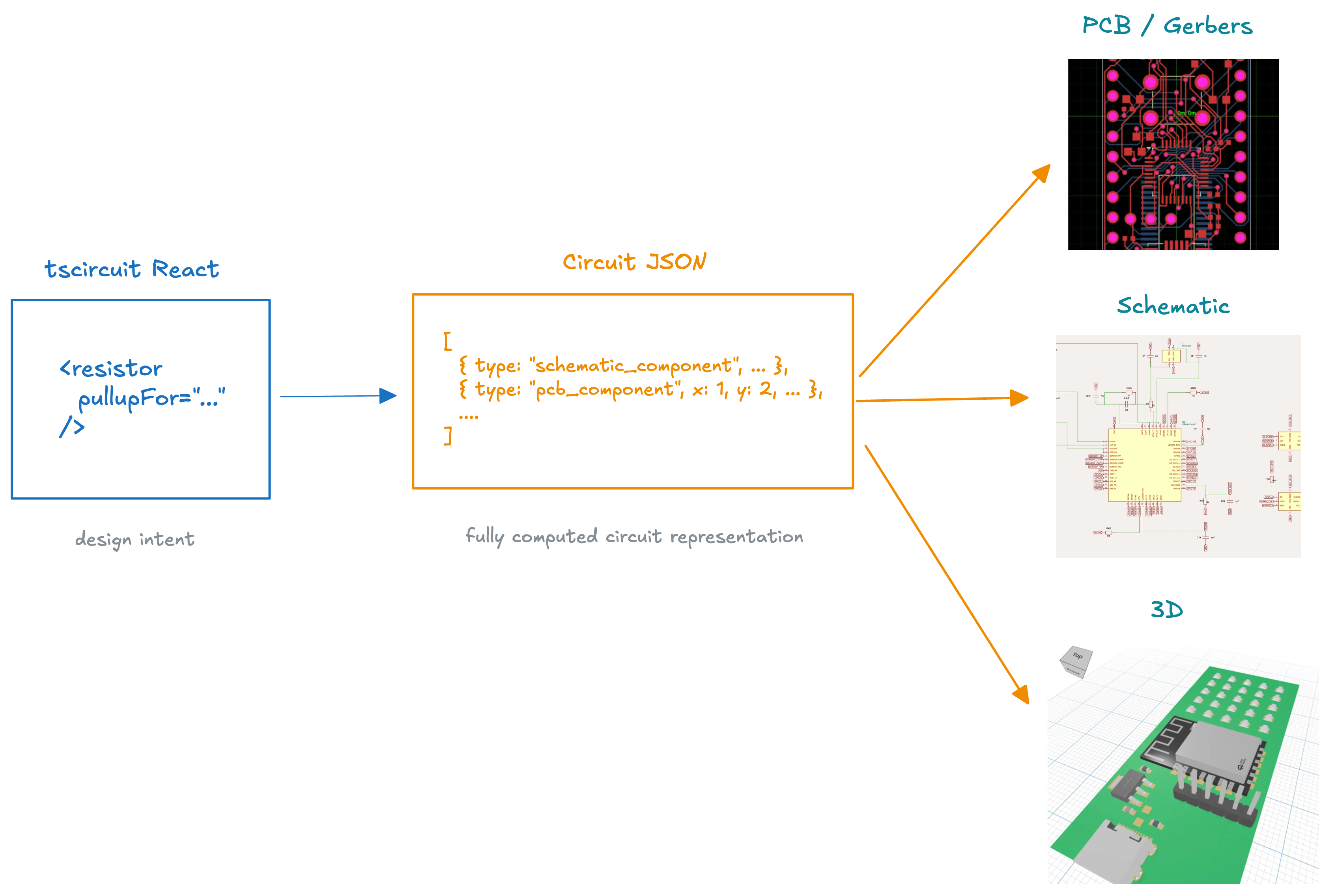
## React: Display all available previews with ``
The `` component is a simple way to display all available
previews for a Circuit JSON array. You can use it by installing the `@tscircuit/runframe`
package and importing it into your `React` project.
```tsx
import { CircuitJsonPreview } from "@tscircuit/runframe"
import { renderToCircuitJson } from "lib/dev/render-to-circuit-json"
export default () => (
,
)}
/>
)
```
You should see something like this:
For more examples and usage, check out the [runframe repo](https://github.com/tscircuit/runframe)
and the [examples directory](https://github.com/tscircuit/runframe/tree/main/examples)!
:::info
Have tscircuit code and want to skip converting to Circuit JSON? Try using the
`` component directly to build your circuit in the browser!
:::
### React: Running tscircuit code in the browser (no Circuit JSON needed!)
The `` component is a simple way to run tscircuit code in the browser.
RunFrame loads the tscircuit runtime (and all the dependencies to build Typescript
code) into a WebWorker and runs the code in the background.
To use RunFrame, you must provide a `fsMap` object. This object maps file paths
to file contents. Files inside this "filesystem map" can import each other, this
is super useful when you have many files to import such as a `manual-edits.json`
file!
```tsx
import { RunFrame } from "@tscircuit/runframe"
export default () => (
)
`,
}}
entrypoint="main.tsx"
/>
)
```
You can see different examples of how RunFrame looks for different circuits
on the [RunFrame online examples page](https://runframe.vercel.app/)
`` automatically handles imports from the tscircuit registry
## Displaying Circuit JSON without React
Are you interested in this? Please [upvote this issue](https://github.com/tscircuit/tscircuit/issues/508)
so we can prioritize it!
---
title: Platform Configuration
description: >-
The Platform Configuration allows you to change tscircuit behavior to best
suit the platform the tscircuit code is running on.
---
## Overview
The Platform Configuration allows you to change tscircuit behavior to best suit
the platform the tscircuit code is running on.
Some use cases:
- Organizations may want to customize the cloud autorouter to avoid sending sensitive designs outside your company
- Organizations may want to introduce custom footprint strings
using a prefix like `footprint="my-company:*"`
- Organizations may want to use their own internal registry for importing circuits instead of [tscircuit.com](https://tscircuit.com)
- For [autorouting.com](https://autorouting.com), we configure the platform to not perform any autorouting
## Customizing the Platform
All of the following features of the platform can be configured:
- **partsEngine** - The engine used to automatically find parts matching component specifications
- **registryApiUrl** - The registry to use, defaults to `https://api.tscircuit.com`. See [Registry API](../../web-apis/the-registry-api.md) for more details
- **cloudAutorouterUrl** - The cloud autorouter to use, defaults to a tscircuit cloud service that uses freerouting
- Disable specific circuit outputs to optimize build times, such as disabling autorouting
- **footprintLibraryMap** - Configure custom prefixes for loading footprint strings from a server. This is how built-in strings like `kicad:*` and `jlcpcb:*` are loaded.
- **printBoardInformationToSilkscreen** - Print the board information to the silkscreen. This includes standard board and platform information like the board name, version etc.
> See the full specification for the [tscircuit platform configuration](https://github.com/tscircuit/props/blob/main/lib/platformConfig.ts)
### The Default Platform
The tscircuit default platform configuration sources parts from multiple vendors
and uses the tscircuit backend for autorouting and `@tsci/*` imports.
Current vendors used for automatic part sourcing:
- [JLCPCB](https://jlcpcb.com)
- Digikey (coming soon!)
- Mouser (coming soon!)
For each vendor, tscircuit populates multiple available chips. This means even
if tscircuit finds parts for a vendor, you don't have to use that vendor!
## Using your Platform
:::info
Want more platform features? Tell us about your use case in [this GitHub Discussion!](https://github.com/orgs/tscircuit/discussions/514)
:::
### Configure a project with `tscircuit.config.ts`
For CLI projects, define a `platformConfig` export in `tscircuit.config.ts` at
the root of your project. This lets every board in the project use the same
parts engine, autorouter, registry, or footprint libraries without passing a
platform object into each circuit manually.
For example, the TI parts engine can define components from Texas Instruments
part data. First install it as a development dependency:
```sh
bun add -D github:tscircuit/ti-parts-engine
```
Then configure it in your project:
```ts title="tscircuit.config.ts"
import { createTiPlatformConfig } from "@tscircuit/ti-parts-engine"
export default {
platformConfig: createTiPlatformConfig(),
}
```
You can now use TI components inside tscircuit with automatically loaded SPICE
and footprints:
(
)`,
}}
/>
### Provide a platform programmatically
When you initialize a `RootCircuit`, you can provide the platform configuration
as the `{ platform }` parameter:
```tsx
import { RootCircuit } from "@tscircuit/core"
const circuit = new RootCircuit({
platform: {
registryApiUrl: "https://my-tscircuit-registry.mycompany.com",
},
})
```
This can also be provided to modules like `@tscircuit/eval` to evaluate tscircuit
code:
```tsx
import { CircuitRunner } from "@tscircuit/eval-webworker"
import myPartsEngine from "./my-parts-engine"
const circuitRunner = new CircuitRunner({
platform: {
partsEngine: myPartsEngine,
},
})
await circuitRunner.execute(`
circuit.add(
)`)
await circuitRunner.renderUntilSettled()
const circuitJson = await circuitRunner.getCircuitJson()
```
:::info
Interested in running the entire tscircuit platform privately inside your company?
We're happy to help! Reach out to **enterprise@tscircuit.com**
:::
---
title: Programmatically Building Circuits
description: Use tscircuit libraries and APIs to generate circuits from scripts or services
---
This guide is about using tscircuit inside of scripts, APIs or inside the browser. Maybe you want to create a website that allows your users drag'n'drop to create custom electronics and turn their designs into real circuits automatically.
For most users, there is no need to programmatically build circuits, you can use the [command line](../../command-line/tsci-dev.md) or the [online editor](../../intro/quickstart-web.md) to build and export your circuits into any supported format.
If you're not using Typescript or prefer a "zero-installation" setup, you can fully build your circuits with complex parameters using the [Registry API](../../web-apis/the-registry-api.md)
## Using `RootCircuit` Directly
`RootCircuit` from `tscircuit` converts React code into [Circuit JSON](https://github.com/tscircuit/circuit-json), a universal intermediary format that represents an electronic device.
Here's an example of how to use `RootCircuit` directly to build a circuit into Circuit JSON:
```tsx
import { RootCircuit } from "tscircuit"
const circuit = new RootCircuit()
circuit.add(
)
await circuit.renderUntilSettled()
console.log(circuit.getCircuitJson())
```
This will output a long [Circuit JSON](https://github.com/tscircuit/circuit-json) array that you can convert into many
other formats or display directly inside a [CircuitJsonPreview](./displaying-circuit-json-on-a-webpage.mdx) component.
## Evaluating Typescript Circuits
`@tscircuit/eval` can be used to evaluate Typescript/React code and
automatically import modules from the tscircuit registry.
```tsx
import { CircuitRunner } from "@tscircuit/eval"
const circuitRunner = new CircuitRunner()
await circuitRunner.execute(`
import { RedLed } from "@tsci/seveibar.red-led"
circuit.add(
)`)
await circuitRunner.renderUntilSettled()
const circuitJson = await circuitRunner.getCircuitJson()
// Display or convert the circuit json to any other format!
```
### Evaluating tscircuit inside a web worker
```tsx
import { createCircuitWebWorker } from "@tscircuit/eval/webworker"
const circuitWebWorker = createCircuitWebWorker()
await circuitWebWorker.execute(`
import { RedLed } from "@tsci/seveibar.red-led"
circuit.add(
)
`)
await circuitWebWorker.renderUntilSettled()
const circuitJson = await circuitWebWorker.getCircuitJson()
```
## Converting Circuit JSON to other formats
You can convert [Circuit JSON](https://github.com/tscircuit/circuit-json) to many
other formats:
- [Gerber files](https://github.com/tscircuit/circuit-json-to-gerber)
- [Specctra DSN Autorouting files](https://github.com/tscircuit/dsn-converter)
- [Pick'n'Place Files](https://github.com/tscircuit/circuit-json-to-pnp-csv)
- [PCB and Schematic SVGs](https://github.com/tscircuit/circuit-to-svg)
- [Bill of Materials](https://github.com/tscircuit/circuit-json-to-bom-csv)
- [SPICE netlists and simulations](https://github.com/tscircuit/circuit-json-to-spice)
---
title: Running tscircuit inside an iframe
description: >-
tscircuit can be evaluated inside an iframe. This makes it easy to embed
snippets on a webpage without complex build systems.
---
## Overview
tscircuit can be evaluated inside an iframe. This makes it easy to embed
snippets on a webpage without complex build systems.
Here's an example of an iframe running a tscircuit snippet:
import { TscircuitIframe } from "../../../src/components/TscircuitIframe"
)`,
}}
entrypoint="main.tsx"
/>
## Running tscircuit inside an iframe
To run tscircuit inside an iframe, perform the following steps:
1. Add an iframe that points to `"https://runframe.tscircuit.com/iframe.html"`
2. Listen for the `runframe_ready_to_receive` message from the iframe
3. Send the code you want to run to the iframe via `postMessage`
Here's a fully working example:
```html
RunFrame Host
```
## React iframe wrapper for tscircuit
An iframe wrapper is available to simplify the process of running tscircuit
inside an iframe. To use it, add the `@tscircuit/runframe` package to your
project and use the [`RunFrameWithIframe` component](https://github.com/tscircuit/runframe/blob/main/lib/components/RunFrameWithIframe/RunFrameWithIframe.tsx) like so:
```tsx
import { RunFrameWithIframe } from "@tscircuit/runframe/iframe"
export default () => (
)`,
}}
entrypoint="main.tsx"
/>
)
```
---
title: Running tscircuit with a script tag
description: Load `tscircuit`'s browser build from a CDN and render a circuit written inside a `
An example of an imported JLCPCB component
After your component has been added to tscircuit, you can import it as a
`@tsci/*` import like this:
```tsx
import { ESP32_WROOM_32DC } from "@tsci/AnasSarkiz.ESP32_WROOM_32DC"
export default () => (
)
```
---
title: Importing from KiCad
sidebar_position: 3
description: You can import KiCad components or projects into tscircuit.
---
## Overview
You can import KiCad components or projects into tscircuit.
:::tip
If you're trying to use a footprint from KiCad's standard libraries, you can skip manual importing and reference it directly with the `kicad:` prefix (e.g. `kicad:Resistor_SMD/R_0402_1005Metric`). See [KiCad Footprints](/footprints/kicad-footprints) for more details.
:::
To import from KiCad, you should understand the different file formats KiCad
uses:
- Files for KiCad components
- `kicad_mod` - PCB footprint file for a single component
- `kicad_sym` - Schematic symbol file for a single component
- Files for KiCad projects
- `kicad_pro` - KiCad project file
- `kicad_pcb` - KiCad PCB board file
- `kicad_sch` - KiCad Schematic board file
:::info
We're still building KiCad import directly into tscircuit.com, stay tuned for
when that's available!
:::
## Importing KiCad Components
Currently the easiest way to import KiCad components is to go to [kicad-component.tscircuit.com](https://kicad-component.tscircuit.com/)
and upload your `kicad_mod` and/or `kicad_sym` file.
### Importing KiCad Components using the CLI
Using tscircuit's [open-source KiCad component converter](https://github.com/tscircuit/kicad-component-converter),
we can convert KiCad files on the command line.
First install the component converter:
```bash
npm install -g kicad-component-converter
```
Next, run the following command to convert your KiCad files:
```bash
# Convert a directory ./my-footprints.pretty to a tscircuit project
kicad-component-converter convert-kicad-directory --input-dir ./my-footprints.pretty --output-dir ./my-tscircuit-footprints
```
### Importing `.kicad_pcb` files directly
You can import a KiCad PCB board file as Circuit JSON and place it inside a
tscircuit board with ``:
```tsx
import { circuitJson } from "./example.kicad_pcb"
circuit.add(
,
)
```
### Importing KiCad Components Programmatically
```bash
bun add kicad-component-converter
```
#### Import `.kicad_mod` files directly
`kicad-component-converter` registers a bundler loader that lets you import KiCad
footprints like any other module inside your tscircuit project:
```tsx
import kicadMod from "./footprint.kicad_mod"
export default () => {
return (
)
}
```
#### Convert KiCad files manually
If you need to do the conversion yourself (for example inside a build script),
you can read the `.kicad_mod` file and pass it through the parser:
```tsx
import { parseKicadModToCircuitJson } from "kicad-component-converter"
import { readFileSync } from "node:fs"
const fileContent = readFileSync("SW_SP3T_PCM13.kicad_mod")
const circuitJson = await parseKicadModToCircuitJson(fileContent)
/* [
* {
* "type": "pcb_smtpad",
* "x": 0.345,
* ...
*/
```
[Circuit JSON](https://github.com/tscircuit/circuit-json) can then be converted
into regular tscircuit modules using [circuit-json-to-tscircuit](https://github.com/tscircuit/circuit-json-to-tscircuit)
---
title: Installing KiCad Libraries
sidebar_position: 4
description: Install KiCad footprint libraries from GitHub and use them in your tscircuit projects with full TypeScript support.
---
## Overview
You can install KiCad footprint libraries directly from GitHub using the `tsci add` or `tsci install` command. This is the easiest way to use existing KiCad footprints in your tscircuit projects, with automatic TypeScript type generation for full IDE support.
## Installation
To install a KiCad library from GitHub, use the `tsci add` command with the repository URL:
```bash
tsci add https://github.com/espressif/kicad-libraries
```

:::tip
`tsci install` is an alias for `tsci add` - both commands work identically.
:::
## What Happens During Installation
When you install a repository containing `.kicad_mod` files, `tsci` will automatically:
1. **Add the package to `package.json`** - The library is added as a dependency
2. **Install in `node_modules`** - The package is downloaded and installed
3. **Detect KiCad footprints** - Scans for `.kicad_mod` files in the repository
4. **Generate TypeScript types** - Creates type definitions in `types/.d.ts`
5. **Configure `tsconfig.json`** - Adds the types directory to `typeRoots`
## Using KiCad Footprints in Your Circuit
After installation, you can import `.kicad_mod` files directly in your circuit code:
```tsx
import kicadMod from "kicad-libraries/footprints/Espressif.pretty/ESP32-S2-MINI-1.kicad_mod"
export default () => {
return (
)
}
```
The imported `kicadMod` can be used directly as the `footprint` prop on components like ``.

## Generated Type Definitions
When you install a KiCad library, `tsci` creates a type definition file in the `types/` directory. For example, installing `kicad-libraries` creates `types/kicad-libraries.d.ts`:
```typescript
declare module "kicad-libraries/footprints/Espressif.pretty/ESP32-S2-MINI-1.kicad_mod" {
const value: string
export default value
}
declare module "kicad-libraries/footprints/Espressif.pretty/ESP32-C3-MINI-1.kicad_mod" {
const value: string
export default value
}
// ... declarations for all .kicad_mod files in the library
```
This provides:
- **Full TypeScript support** - No type errors when importing `.kicad_mod` files
- **IDE autocomplete** - Your editor can suggest available footprint paths
- **Import validation** - Catch typos in import paths at compile time
## tsconfig.json Configuration
The command automatically updates your `tsconfig.json` to include the types directory:
```json
{
"compilerOptions": {
"typeRoots": ["./types", "./node_modules/@types"]
}
}
```
If your project doesn't have a `tsconfig.json`, one will be created with the necessary configuration.
## See Also
- [Importing from KiCad](/guides/importing-modules-and-chips/importing-from-kicad) - Other methods to import KiCad components
- [KiCad Footprints](/footprints/kicad-footprints) - Using KiCad's standard library footprints with the `kicad:` prefix
- [tsci add](/command-line/tsci-add) - Installing tscircuit registry packages
---
title: Exporting a KiCad Library
description: >-
Export your tscircuit designs as a KiCad library containing symbols,
footprints, and 3D models that can be reused across multiple KiCad projects.
---
## Overview
tscircuit allows you to export your circuit designs as a **KiCad Library**. Unlike the KiCad Project export (which creates a complete project file), the KiCad Library export creates reusable components that can be imported into any KiCad project.
The exported library includes:
- **Symbol Libraries** (`symbols/` folder) - Schematic symbols for all components
- **Footprint Libraries** (`footprints/` folder) - PCB footprints for all components
- **3D Models** (`3dmodels/` folder) - 3D model files (STEP/WRL) referenced by footprints
- **Library Tables** (`fp-lib-table`, `sym-lib-table`) - Configuration files for KiCad
## User vs Builtin Components
tscircuit automatically separates your components into two library categories:
### User Components
Components that use **custom footprints or symbols** are placed in the user library, named after your project (e.g., `my-library`). These include:
- Components with a custom `footprint` prop (JSX footprint definition):
```tsx
}
/>
```
- Components with a custom `symbol` prop (JSX symbol definition):
```tsx
}
/>
```
### Builtin Components
Components that use **standard footprinter strings** (e.g., `0402`, `soic8`) are placed in the `tscircuit_builtin` library. This includes all footprints that tscircuit supports by default.
## Directory Structure
```
my-library/
├── symbols/
│ ├── my-library.kicad_sym # User symbols (custom symbols)
│ └── tscircuit_builtin.kicad_sym # Builtin symbols (standard symbols)
├── footprints/
│ ├── my-library.pretty/ # User footprints
│ │ └── MyCustomSwitch.kicad_mod
│ └── tscircuit_builtin.pretty/ # Builtin footprints
│ ├── resistor_0402.kicad_mod
│ └── chip_soic8.kicad_mod
├── 3dmodels/
│ └── switch.step
├── fp-lib-table
└── sym-lib-table
```
## How to Export
### Using the Browser
1. Run `tsci dev` in your project directory
2. Navigate to **File > Export > KiCad Library**
3. A zip file will be downloaded containing all library files
### Using the CLI
```bash
tsci export ./lib/my-library.ts -f kicad-library
```
The CLI will:
1. Discover all component exports from the entry file
2. Build each component to circuit JSON
3. Extract and classify footprints/symbols (user vs builtin)
4. Generate the KiCad library files
## Using the Library in KiCad
1. **Extract/Copy the library** to your KiCad project folder or a shared libraries location
2. **Add the library tables** to your KiCad project:
- Copy `fp-lib-table` and `sym-lib-table` to your project folder, OR
- Merge the entries into your existing library tables
3. **Use the symbols and footprints** in your schematic and PCB:
- Custom symbols appear under your library name (e.g., `my-library`)
- Standard symbols appear under `tscircuit_builtin`
## Including 3D Models
Add a `cadModel` prop to include 3D models in your export:
```tsx
import stepUrl from "./switch.step"
}
/>
```
The 3D model will be:
- Referenced in the footprint file with the correct path
- Included in the `3dmodels/` folder of the export
---
title: KiCad Metadata
sidebar_position: 1
description: Document KiCad-specific metadata for footprints and symbols on tscircuit components
---
# KiCad Metadata
tscircuit components support KiCad-specific metadata properties that preserve information from KiCad footprint and symbol files. These properties are available on all normal components (chip, resistor, capacitor, etc.) and are useful when importing from KiCad or when you need to include KiCad-specific information in your exported designs.
## Properties Overview
| Property | Element | Description |
|----------|---------|-------------|
| `kicadFootprintMetadata` | Components | Metadata from KiCad footprint (`.kicad_mod`) files |
| `kicadSymbolMetadata` | Components | Metadata from KiCad symbol (`.kicad_sym`) files |
| `kicadPinMetadata` | `` | Metadata for KiCad pin electrical and visual properties |
---
## kicadFootprintMetadata
The `kicadFootprintMetadata` property stores metadata extracted from KiCad footprint files. This includes information about the footprint's properties, attributes, pads, and 3D model.
### Type Definition
```typescript
interface KicadFootprintMetadata {
footprintName?: string
version?: number | string
generator?: string
generatorVersion?: number | string
layer?: string
properties?: KicadFootprintProperties
attributes?: KicadFootprintAttributes
pads?: KicadFootprintPad[]
embeddedFonts?: boolean
model?: KicadFootprintModel
}
```
### Properties
#### Top-level Properties
| Property | Type | Description |
|----------|------|-------------|
| `footprintName` | `string` | Name identifier for the footprint |
| `version` | `number \| string` | KiCad file format version |
| `generator` | `string` | Tool that generated the footprint |
| `generatorVersion` | `number \| string` | Version of the generator tool |
| `layer` | `string` | Default layer (e.g., `"F.Cu"`) |
| `embeddedFonts` | `boolean` | Whether fonts are embedded in the footprint |
#### properties
Standard KiCad footprint properties for documentation:
```typescript
interface KicadFootprintProperties {
Reference?: KicadProperty // Component reference designator (e.g., "R1")
Value?: KicadProperty // Component value (e.g., "10k")
Datasheet?: KicadProperty // Link to component datasheet
Description?: KicadProperty // Human-readable description
}
interface KicadProperty {
value: string
at?: { x: number | string; y: number | string; rotation?: number | string }
layer?: string
uuid?: string
hide?: boolean
effects?: {
font?: {
size?: { x: number | string; y: number | string }
thickness?: number | string
}
}
}
```
#### attributes
Footprint manufacturing attributes:
```typescript
interface KicadFootprintAttributes {
through_hole?: boolean // THT component
smd?: boolean // SMD component
exclude_from_pos_files?: boolean // Exclude from pick-and-place
exclude_from_bom?: boolean // Exclude from bill of materials
}
```
#### pads
Array of pad definitions:
```typescript
interface KicadFootprintPad {
name: string // Pad name/number
type: string // Pad type (e.g., "smd", "thru_hole")
shape?: string // Pad shape (e.g., "rect", "circle", "oval")
at?: { x: number | string; y: number | string; rotation?: number | string }
size?: { x: number | string; y: number | string }
drill?: number | string // Drill diameter for THT pads
layers?: string[] // Copper layers (e.g., ["F.Cu", "F.Paste"])
removeUnusedLayers?: boolean
uuid?: string
}
```
#### model
3D model reference and transforms:
```typescript
interface KicadFootprintModel {
path: string // Path to 3D model file
offset?: { x: number | string; y: number | string; z: number | string }
scale?: { x: number | string; y: number | string; z: number | string }
rotate?: { x: number | string; y: number | string; z: number | string }
}
```
### Example Usage
```tsx
```
---
## kicadSymbolMetadata
The `kicadSymbolMetadata` property stores metadata extracted from KiCad symbol files. This includes schematic-specific information like pin configuration, BOM settings, and symbol properties.
### Type Definition
```typescript
interface KicadSymbolMetadata {
symbolName?: string
extends?: string
pinNumbers?: KicadSymbolPinNumbers
pinNames?: KicadSymbolPinNames
excludeFromSim?: boolean
inBom?: boolean
onBoard?: boolean
properties?: KicadSymbolProperties
embeddedFonts?: boolean
}
```
### Properties
#### Top-level Properties
| Property | Type | Description |
|----------|------|-------------|
| `symbolName` | `string` | Symbol identifier name |
| `extends` | `string` | Parent symbol for inheritance |
| `excludeFromSim` | `boolean` | Exclude from SPICE simulation |
| `inBom` | `boolean` | Include in bill of materials |
| `onBoard` | `boolean` | Component appears on PCB |
| `embeddedFonts` | `boolean` | Whether fonts are embedded |
#### pinNumbers
Pin number display configuration:
```typescript
interface KicadSymbolPinNumbers {
hide?: boolean // Hide pin numbers in schematic
}
```
#### pinNames
Pin name display configuration:
```typescript
interface KicadSymbolPinNames {
offset?: number | string // Distance from pin to name text
hide?: boolean // Hide pin names in schematic
}
```
#### properties
Standard KiCad symbol properties:
```typescript
interface KicadSymbolProperties {
Reference?: KicadSymbolProperty // Reference designator prefix (e.g., "U")
Value?: KicadSymbolProperty // Component value/name
Footprint?: KicadSymbolProperty // Associated footprint
Datasheet?: KicadSymbolProperty // Datasheet URL
Description?: KicadSymbolProperty // Human-readable description
ki_keywords?: KicadSymbolProperty // Search keywords
ki_fp_filters?: KicadSymbolProperty // Footprint filter patterns
}
interface KicadSymbolProperty {
value: string
id?: number | string
at?: { x: number | string; y: number | string; rotation?: number | string }
effects?: {
font?: {
size?: { x: number | string; y: number | string }
thickness?: number | string
}
justify?: string | string[]
hide?: boolean
}
}
```
### Example Usage
```tsx
```
---
## kicadPinMetadata
The `kicadPinMetadata` property is used on `` elements to store KiCad-specific pin information. This includes the pin's electrical type, graphic style, and text sizing properties that are used when exporting to KiCad symbol files.
### Type Definition
```typescript
interface KicadPinMetadata {
electricalType?: KicadPinElectricalType
graphicStyle?: KicadPinGraphicStyle
pinLength?: Distance
nameTextSize?: Distance
numberTextSize?: Distance
}
```
### Properties
| Property | Type | Description |
|----------|------|-------------|
| `electricalType` | `KicadPinElectricalType` | Electrical characteristics of the pin |
| `graphicStyle` | `KicadPinGraphicStyle` | Visual representation style of the pin |
| `pinLength` | `Distance` | Physical length of the pin |
| `nameTextSize` | `Distance` | Text size for the pin name label |
| `numberTextSize` | `Distance` | Text size for the pin number label |
#### electricalType
Specifies the electrical characteristics of the pin:
| Value | Description |
|-------|-------------|
| `"input"` | Input pin |
| `"output"` | Output pin |
| `"bidirectional"` | Bidirectional pin |
| `"tri_state"` | Tri-state pin |
| `"passive"` | Passive pin (resistors, capacitors, etc.) |
| `"free"` | Free pin (can connect to anything) |
| `"unspecified"` | Unspecified electrical type |
| `"power_in"` | Power input pin (VCC, GND) |
| `"power_out"` | Power output pin |
| `"open_collector"` | Open collector output |
| `"open_emitter"` | Open emitter output |
| `"no_connect"` | No connection pin |
#### graphicStyle
Defines the visual representation of the pin in schematics:
| Value | Description |
|-------|-------------|
| `"line"` | Simple line (default) |
| `"inverted"` | Inverted (bubble) |
| `"clock"` | Clock input indicator |
| `"inverted_clock"` | Inverted clock |
| `"input_low"` | Active low input |
| `"clock_low"` | Active low clock |
| `"output_low"` | Active low output |
| `"falling_edge_clock"` | Falling edge triggered clock |
| `"nonlogic"` | Non-logic pin |
### Example Usage
```tsx
```
---
## When to Use KiCad Metadata
### Importing from KiCad
When you [import components from KiCad](/guides/importing-modules-and-chips/importing-from-kicad), the converter tools automatically populate these metadata properties. This preserves the original KiCad information for reference and export compatibility.
### Exporting to KiCad
When exporting your tscircuit design to KiCad format, these metadata properties are used to generate accurate `.kicad_mod` and `.kicad_sym` files that maintain compatibility with KiCad workflows.
## Related Documentation
- [Importing from KiCad](/guides/importing-modules-and-chips/importing-from-kicad) - How to import KiCad components
- [KiCad Footprints](/footprints/kicad-footprints) - Using KiCad footprints with the `kicad:` prefix
- [Installing KiCad Libraries](/guides/importing-modules-and-chips/installing-kicad-libraries-from-github) - Adding KiCad libraries to your project
---
title: Using tscircuit KiCad PCM URLs
description: >-
Install tscircuit component libraries directly into KiCad using the Plugin and
Content Manager (PCM) with cloud-hosted repository URLs.
---
## Overview
tscircuit packages can be installed directly into KiCad using the **Plugin and Content Manager (PCM)**. Each published tscircuit package includes a KiCad PCM URL that points to a repository hosted on `tscircuit.app` containing the symbols, footprints, and 3D models for all components in the package.
This guide walks you through the process of adding a tscircuit package to KiCad using the PCM URL.
## Step 1: Find the KiCad PCM URL
Navigate to your tscircuit package page on [tscircuit.com](https://tscircuit.com). In the **Releases** section on the right sidebar, you'll find a **KiCad PCM URL** link. If you don't see this link, enable `kicadPcm` in your tscircuit config (see [tscircuit config](https://docs.tscircuit.com/guides/tscircuit-essentials/tscircuit-config)).

## Step 2: Copy the Repository URL
Click the **KiCad PCM URL** link to open the repository JSON file in your browser. Copy the full URL from the address bar.

## Step 3: Add the Repository in KiCad PCM
1. Open KiCad and go to **Tools > Plugin and Content Manager**
2. Click the **Manage...** button in the top-right corner
3. In the "Manage Repositories" dialog, click the **+** button to add a new repository
4. Paste the repository URL you copied and click **OK**
5. Click **Save** to save the repository configuration

## Step 4: Select the Repository
After saving, use the repository dropdown at the top-left of the PCM window to select your newly added tscircuit repository.

## Step 5: Install the Library
1. Navigate to the **Libraries** tab
2. Select the tscircuit library package from the list
3. Click the **Install** button
4. Click **Apply Pending Changes** at the bottom of the window to begin the installation

The download progress will be displayed:

## Step 6: Verify Installation
Once the installation is complete, switch to the **Installed** tab to verify that the library appears in your installed packages list.

## Step 7: Use the Library in Your Project
The library is now ready to use in your KiCad projects. Open the **Schematic Editor** and use **Add Symbol** (shortcut: `A`) to browse and place components from the installed library.
The components will appear under a library name prefixed with `PCM_` (e.g., `PCM_jlc100`).

---
title: Measuring circuit size using scripts
description: Use @tscircuit/core to evaluate groups, extract bounding boxes, and pick board templates that fit
---
Automating board design often starts with a question: _how much space does this group of parts actually need?_ This guide shows how to render groups inside a script, capture their dimensions, and store metadata that other steps in your pipeline can read.
## Recommended workflow
1. Keep each reusable group in a `design-groups/` directory so it can be evaluated on its own.
2. Run a script that loads every group, renders it with `tscircuit`, and saves a metadata JSON file containing width and height.
3. When you build the final board component, import the metadata file to decide which carrier template has enough room.
Separating generated metadata from hand-authored TSX keeps the process debuggable. If you _do_ write metadata back into a `.tsx` file, wrap the generated block in clearly marked comments so humans and tools know where automation can safely write.
## Directory layout
```text
my-project/
├─ design-groups/
│ ├─ esp32-breakout.tsx # Exports the group you want to analyze
│ └─ esp32-breakout.metadata.json # Width/height baked by the script
├─ carriers/
│ └─ esp32-breakout-carrier.tsx # Imports metadata when building the final board
└─ scripts/
└─ bake-group-metadata.ts # Script that renders the group and writes JSON
```
Each group file should export a React component that renders a `` inside a `` or within the structure you normally use. The script can then import it, render it in isolation, and evaluate the results.
```tsx title="design-groups/esp32-breakout.tsx"
export const Esp32Breakout = () => (
{/* Components, nets, and layout props */}
)
```
## Rendering a group and measuring its bounding box
The snippet below renders a group, waits for placement to settle, and then extracts the PCB group bounds from Circuit JSON.
```tsx
import { RootCircuit } from "tscircuit"
import { Esp32Breakout } from "../design-groups/esp32-breakout"
const circuit = new RootCircuit()
circuit.add(
)
await circuit.renderUntilSettled();
const circuitJson = await circuit.getCircuitJson();
const rootGroupOrBoard = circuitJson.find(
(item) =>
item.type === "pcb_board" ||
(item.type === "pcb_group" && item.is_subcircuit),
);
Bun.write("../design-groups/esp32-breakout.metadata.json", JSON.stringify(rootGroupOrBoard, null, 2));
```
You can do this dynamically for every file in the `design-groups` directory:
```tsx
import { RootCircuit } from "tscircuit"
for (const file of await Bun.glob("design-groups/*.tsx")) {
const { default: GroupComponent } = await import(`../${file}`);
const groupName = file.split("/").pop()?.replace(".tsx", "");
const circuit = new RootCircuit();
circuit.add();
await circuit.renderUntilSettled();
const circuitJson = await circuit.getCircuitJson();
const rootGroupOrBoard = circuitJson.find(
(item) =>
item.type === "pcb_board" ||
(item.type === "pcb_group" && item.is_subcircuit),
);
await Bun.write(
`../design-groups/${groupName}.metadata.json`,
JSON.stringify(rootGroupOrBoard, null, 2)
);
}
```
## Detecting packing failures programmatically
Packing issues (such as overlaps or components outside the board) are surfaced in Circuit JSON as elements whose `type` ends in `_error`, for example `pcb_placement_error`, `pcb_footprint_overlap_error`, and `pcb_component_outside_board_error`. You can scan for them before trusting the bounding box.
```ts
function getPackingErrors(json: CircuitJson) {
return json.filter(
(element) =>
element.type.startsWith("pcb_") && element.type.endsWith("_error"),
)
}
```
If `getPackingErrors` returns any elements, skip writing metadata and log the error messages so you can debug the group in isolation. You can also persist the raw JSON to disk for later inspection or feed it into tools like `circuitjson.com`.
## Trying candidate board sizes
Once you can render a group programmatically, you can try it against a list of candidate board footprints and pick the smallest one that succeeds. Render the group inside a `` that has the candidate size, check for packing errors, and return the first success.
```tsx
const CANDIDATE_SIZES = [
{ name: "SMALL", width: 21, height: 51 },
{ name: "MEDIUM", width: 24, height: 58 },
]
async function findSmallestBoard(load: () => Promise) {
for (const size of CANDIDATE_SIZES) {
const circuit = new RootCircuit()
const Circuit = await load()
circuit.add(
,
)
await circuit.renderUntilSettled()
const json = (await circuit.getCircuitJson()) as CircuitJson
if (getPackingErrors(json).length === 0) {
return { size, json }
}
}
throw new Error("No candidate board size could pack the circuit")
}
```
With this helper you can run multiple passes: one to bake metadata for inspection, and another to select the best board footprint automatically. Store the selected board ID alongside the size metadata so later steps (such as generating headers or enclosure geometry) can read the decision without re-running the analysis.
## Using the baked metadata in a board component
The final board component can import the JSON and pick a template accordingly. Because the metadata is static, you can safely load it during module evaluation.
```tsx
import metadata from "../design-groups/esp32-breakout.metadata.json" assert { type: "json" }
const TEMPLATE_OPTIONS = [
{ id: "SMALL", width: 21, height: 51 },
{ id: "MEDIUM", width: 24, height: 58 },
]
const selectedTemplate = TEMPLATE_OPTIONS.find(
(option) =>
option.width >= metadata.width && option.height >= metadata.height,
)
if (!selectedTemplate) {
throw new Error("No board template can fit the baked group bounds")
}
export const Esp32BreakoutCarrier = ({ children }: { children: React.ReactNode }) => (
{children}
)
```
When automation needs to update the layout (for example, after rerunning packing with AI assistance), rerun the baking script to regenerate the JSON and let the board component pick a new template automatically. This keeps generated numbers out of your hand-authored TSX while remaining easy to audit.
You can add a script inside your package.json file to run the baking script:
```json
{
"scripts": {
"bake-metadata": "bun run scripts/bake-metadata.ts"
}
}
```
---
title: Building a Static Site
description: "`tsci build --site` packages your tscircuit project into a static website that anyone can browse without running a server."
---
`tsci build --site` packages your tscircuit project into a static website that anyone can browse without running a server. The command evaluates your circuits, exports the generated assets into a `dist` folder, and wires them up to the tscircuit RunFrame viewer so visitors can flip between PCB, schematic, and 3D previews right in the browser.
The [Common tscircuit gallery](https://common.tscircuit.com/) is an example of a site generated with this workflow.
## Prerequisites
Before building a site, make sure you have:
- A tscircuit project with one or more `*.circuit.tsx` files or another supported entrypoint.
- The tscircuit CLI installed (`npm install -g tsci`, `bunx tsci`, or `npx tsci`).
- Any dependencies that your circuits import (registry components, local packages, etc.).
## Building the site
Run the build command from the root of your project:
```bash
# generates dist/index.html and other assets
npx tsci build --site
```
The CLI resolves your entrypoint, evaluates every circuit, and then writes a static site to `dist/site/` alongside the usual `dist/circuit.json` outputs. The generated folder contains:
- `index.html` – a ready-to-host viewer.
- `lib/…/circuit.json` – one JSON file per design so the viewer can lazy load each project.
- Supporting JavaScript, CSS, and WebAssembly bundles for the RunFrame UI.
You can inspect the result locally with any static file server, for example:
```bash
npx serve dist
```
Opening `http://localhost:3000` (or the port reported by your static server) shows the same interactive viewer experience used at common.tscircuit.com.
## Customizing the catalog
The site automatically lists every circuit that `tsci build` evaluates. If you already use a `tscircuit.config.json` file, the same settings shape the static catalog: `mainEntrypoint` lets you pick a custom starting file, and the existing include/exclude patterns limit which `*.circuit.tsx` sources are exported.
When you add extra documentation or screenshots, keep them in a public asset folder (for example `public/`), then point to them from your circuits. Static assets referenced at build time are copied into `dist` so they ship with the site bundle.
## Deploying to Vercel
Vercel can host the generated site without any special adapters:
1. Push your project to GitHub or GitLab.
2. Create a new Vercel project that points to the repository.
3. Set the **Build Command** to `npx tsci build --site` (or `bunx tsci build --site` if you prefer Bun).
4. Set the **Output Directory** to `dist`.
5. Trigger a deploy – Vercel runs the build, uploads the static folder, and serves it on your chosen domain.
For preview deployments, Vercel repeats these steps on every pull request so reviewers can browse the circuits before merging.
## Deploying elsewhere
Because the output is plain HTML/JS/CSS, you can host it almost anywhere:
- **GitHub Pages** – run `npx tsci build --site` in CI and publish the `dist` folder to `gh-pages`.
- **Netlify** – configure the build command and output directory just like Vercel.
- **S3/CloudFront or static buckets** – upload the generated files with `aws s3 sync dist s3://your-bucket`.
Once deployed, the site stays fast and inexpensive to serve because no server-side rendering or API proxy is required—the viewer fetches the prebuilt `circuit.json` files directly from storage.
---
title: Connect GitHub Repositories to tscircuit
description: Link your project repo to tscircuit for automatic previews and publishing
---
You can connect your GitHub repositories to tscircuit to automatically
publish updates, access instant previews and make sharing boards easier.
You'll want to use the [command line tool](../../intro/quickstart-cli.md) to initialize
an application and push to tscircuit.com using [`tsci push`](../../command-line/tsci-push.md)
After that, navigate to the tscircuit.com page for your circuit and click "Connect to GitHub"
button on the right side of the page.

After connecting to GitHub, every time you merge a small GitHub action will
run to update the circuit on tscircuit.com. You

---
title: Displaying Circuit JSON on a Webpage
description: Render Circuit JSON in web apps using RunFrame and related components
---
[Circuit JSON](https://github.com/tscircuit/circuit-json) is a universal
intermediary format for representing an electronic circuit. It contains PCB,
Schematic, 3D, Bill of Materials and simulation information.
tscircuit code always converts into Circuit JSON, which can be displayed in
any of our React components
:::tip
You can also upload your Circuit JSON to [circuitjson.com](https://circuitjson.com)
for a quick preview!
:::

## React: Display all available previews with ``
The `` component is a simple way to display all available
previews for a Circuit JSON array. You can use it by installing the `@tscircuit/runframe`
package and importing it into your `React` project.
```tsx
import { CircuitJsonPreview } from "@tscircuit/runframe"
import { renderToCircuitJson } from "lib/dev/render-to-circuit-json"
export default () => (
,
)}
/>
)
```
You should see something like this:

For more examples and usage, check out the [runframe repo](https://github.com/tscircuit/runframe)
and the [examples directory](https://github.com/tscircuit/runframe/tree/main/examples)!
:::info
Have tscircuit code and want to skip converting to Circuit JSON? Try using the
`` component directly to build your circuit in the browser!
:::
### React: Running tscircuit code in the browser (no Circuit JSON needed!)
The `` component is a simple way to run tscircuit code in the browser.
RunFrame loads the tscircuit runtime (and all the dependencies to build Typescript
code) into a WebWorker and runs the code in the background.
To use RunFrame, you must provide a `fsMap` object. This object maps file paths
to file contents. Files inside this "filesystem map" can import each other, this
is super useful when you have many files to import such as a `manual-edits.json`
file!
```tsx
import { RunFrame } from "@tscircuit/runframe"
export default () => (
)
`,
}}
entrypoint="main.tsx"
/>
)
```
You can see different examples of how RunFrame looks for different circuits
on the [RunFrame online examples page](https://runframe.vercel.app/)
`` automatically handles imports from the tscircuit registry
## Displaying Circuit JSON without React
Are you interested in this? Please [upvote this issue](https://github.com/tscircuit/tscircuit/issues/508)
so we can prioritize it!
---
title: Platform Configuration
description: >-
The Platform Configuration allows you to change tscircuit behavior to best
suit the platform the tscircuit code is running on.
---
## Overview
The Platform Configuration allows you to change tscircuit behavior to best suit
the platform the tscircuit code is running on.
Some use cases:
- Organizations may want to customize the cloud autorouter to avoid sending sensitive designs outside your company
- Organizations may want to introduce custom footprint strings
using a prefix like `footprint="my-company:*"`
- Organizations may want to use their own internal registry for importing circuits instead of [tscircuit.com](https://tscircuit.com)
- For [autorouting.com](https://autorouting.com), we configure the platform to not perform any autorouting
## Customizing the Platform
All of the following features of the platform can be configured:
- **partsEngine** - The engine used to automatically find parts matching component specifications
- **registryApiUrl** - The registry to use, defaults to `https://api.tscircuit.com`. See [Registry API](../../web-apis/the-registry-api.md) for more details
- **cloudAutorouterUrl** - The cloud autorouter to use, defaults to a tscircuit cloud service that uses freerouting
- Disable specific circuit outputs to optimize build times, such as disabling autorouting
- **footprintLibraryMap** - Configure custom prefixes for loading footprint strings from a server. This is how built-in strings like `kicad:*` and `jlcpcb:*` are loaded.
- **printBoardInformationToSilkscreen** - Print the board information to the silkscreen. This includes standard board and platform information like the board name, version etc.
> See the full specification for the [tscircuit platform configuration](https://github.com/tscircuit/props/blob/main/lib/platformConfig.ts)
### The Default Platform
The tscircuit default platform configuration sources parts from multiple vendors
and uses the tscircuit backend for autorouting and `@tsci/*` imports.
Current vendors used for automatic part sourcing:
- [JLCPCB](https://jlcpcb.com)
- Digikey (coming soon!)
- Mouser (coming soon!)
For each vendor, tscircuit populates multiple available chips. This means even
if tscircuit finds parts for a vendor, you don't have to use that vendor!
## Using your Platform
:::info
Want more platform features? Tell us about your use case in [this GitHub Discussion!](https://github.com/orgs/tscircuit/discussions/514)
:::
### Configure a project with `tscircuit.config.ts`
For CLI projects, define a `platformConfig` export in `tscircuit.config.ts` at
the root of your project. This lets every board in the project use the same
parts engine, autorouter, registry, or footprint libraries without passing a
platform object into each circuit manually.
For example, the TI parts engine can define components from Texas Instruments
part data. First install it as a development dependency:
```sh
bun add -D github:tscircuit/ti-parts-engine
```
Then configure it in your project:
```ts title="tscircuit.config.ts"
import { createTiPlatformConfig } from "@tscircuit/ti-parts-engine"
export default {
platformConfig: createTiPlatformConfig(),
}
```
You can now use TI components inside tscircuit with automatically loaded SPICE
and footprints:
(
)`,
}}
/>
### Provide a platform programmatically
When you initialize a `RootCircuit`, you can provide the platform configuration
as the `{ platform }` parameter:
```tsx
import { RootCircuit } from "@tscircuit/core"
const circuit = new RootCircuit({
platform: {
registryApiUrl: "https://my-tscircuit-registry.mycompany.com",
},
})
```
This can also be provided to modules like `@tscircuit/eval` to evaluate tscircuit
code:
```tsx
import { CircuitRunner } from "@tscircuit/eval-webworker"
import myPartsEngine from "./my-parts-engine"
const circuitRunner = new CircuitRunner({
platform: {
partsEngine: myPartsEngine,
},
})
await circuitRunner.execute(`
circuit.add(
)`)
await circuitRunner.renderUntilSettled()
const circuitJson = await circuitRunner.getCircuitJson()
```
:::info
Interested in running the entire tscircuit platform privately inside your company?
We're happy to help! Reach out to **enterprise@tscircuit.com**
:::
---
title: Programmatically Building Circuits
description: Use tscircuit libraries and APIs to generate circuits from scripts or services
---
This guide is about using tscircuit inside of scripts, APIs or inside the browser. Maybe you want to create a website that allows your users drag'n'drop to create custom electronics and turn their designs into real circuits automatically.
For most users, there is no need to programmatically build circuits, you can use the [command line](../../command-line/tsci-dev.md) or the [online editor](../../intro/quickstart-web.md) to build and export your circuits into any supported format.
If you're not using Typescript or prefer a "zero-installation" setup, you can fully build your circuits with complex parameters using the [Registry API](../../web-apis/the-registry-api.md)
## Using `RootCircuit` Directly
`RootCircuit` from `tscircuit` converts React code into [Circuit JSON](https://github.com/tscircuit/circuit-json), a universal intermediary format that represents an electronic device.
Here's an example of how to use `RootCircuit` directly to build a circuit into Circuit JSON:
```tsx
import { RootCircuit } from "tscircuit"
const circuit = new RootCircuit()
circuit.add(
)
await circuit.renderUntilSettled()
console.log(circuit.getCircuitJson())
```
This will output a long [Circuit JSON](https://github.com/tscircuit/circuit-json) array that you can convert into many
other formats or display directly inside a [CircuitJsonPreview](./displaying-circuit-json-on-a-webpage.mdx) component.
## Evaluating Typescript Circuits
`@tscircuit/eval` can be used to evaluate Typescript/React code and
automatically import modules from the tscircuit registry.
```tsx
import { CircuitRunner } from "@tscircuit/eval"
const circuitRunner = new CircuitRunner()
await circuitRunner.execute(`
import { RedLed } from "@tsci/seveibar.red-led"
circuit.add(
)`)
await circuitRunner.renderUntilSettled()
const circuitJson = await circuitRunner.getCircuitJson()
// Display or convert the circuit json to any other format!
```
### Evaluating tscircuit inside a web worker
```tsx
import { createCircuitWebWorker } from "@tscircuit/eval/webworker"
const circuitWebWorker = createCircuitWebWorker()
await circuitWebWorker.execute(`
import { RedLed } from "@tsci/seveibar.red-led"
circuit.add(
)
`)
await circuitWebWorker.renderUntilSettled()
const circuitJson = await circuitWebWorker.getCircuitJson()
```
## Converting Circuit JSON to other formats
You can convert [Circuit JSON](https://github.com/tscircuit/circuit-json) to many
other formats:
- [Gerber files](https://github.com/tscircuit/circuit-json-to-gerber)
- [Specctra DSN Autorouting files](https://github.com/tscircuit/dsn-converter)
- [Pick'n'Place Files](https://github.com/tscircuit/circuit-json-to-pnp-csv)
- [PCB and Schematic SVGs](https://github.com/tscircuit/circuit-to-svg)
- [Bill of Materials](https://github.com/tscircuit/circuit-json-to-bom-csv)
- [SPICE netlists and simulations](https://github.com/tscircuit/circuit-json-to-spice)
---
title: Running tscircuit inside an iframe
description: >-
tscircuit can be evaluated inside an iframe. This makes it easy to embed
snippets on a webpage without complex build systems.
---
## Overview
tscircuit can be evaluated inside an iframe. This makes it easy to embed
snippets on a webpage without complex build systems.
Here's an example of an iframe running a tscircuit snippet:
import { TscircuitIframe } from "../../../src/components/TscircuitIframe"
)`,
}}
entrypoint="main.tsx"
/>
## Running tscircuit inside an iframe
To run tscircuit inside an iframe, perform the following steps:
1. Add an iframe that points to `"https://runframe.tscircuit.com/iframe.html"`
2. Listen for the `runframe_ready_to_receive` message from the iframe
3. Send the code you want to run to the iframe via `postMessage`
Here's a fully working example:
```html
RunFrame Host
```
## React iframe wrapper for tscircuit
An iframe wrapper is available to simplify the process of running tscircuit
inside an iframe. To use it, add the `@tscircuit/runframe` package to your
project and use the [`RunFrameWithIframe` component](https://github.com/tscircuit/runframe/blob/main/lib/components/RunFrameWithIframe/RunFrameWithIframe.tsx) like so:
```tsx
import { RunFrameWithIframe } from "@tscircuit/runframe/iframe"
export default () => (
)`,
}}
entrypoint="main.tsx"
/>
)
```
---
title: Running tscircuit with a script tag
description: Load `tscircuit`'s browser build from a CDN and render a circuit written inside a `